R
DC and Switching Characteristics
To create a Xilinx MySupport user account and sign up for automatic
•Sign Up for Alerts on Xilinx MySupport
www.xilinx.com/xlnx/xil_ans_display.jsp?getPagePath=19380
Timing parameters and their representative values are selected for inclusion below either because they are important as general design requirements or they indicate fundamental device performance characteristics. The
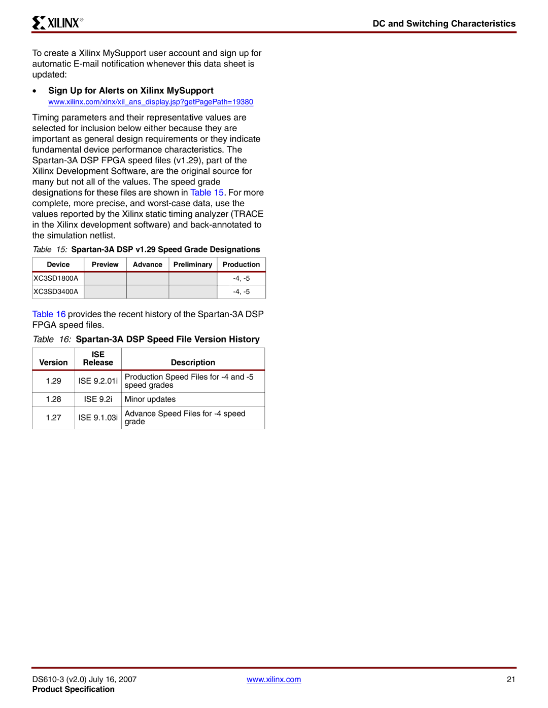
Table 15: Spartan-3A DSP v1.29 Speed Grade Designations
Device | Preview | Advance | Preliminary | Production |
XC3SD1800A |
|
|
| |
|
|
|
|
|
XC3SD3400A |
|
|
| |
|
|
|
|
|
Table 16 provides the recent history of the
FPGA speed files.
Table 16: Spartan-3A DSP Speed File Version History
| ISE |
|
Version | Release | Description |
1.29 | ISE 9.2.01i | Production Speed Files for |
|
| speed grades |
1.28 | ISE 9.2i | Minor updates |
|
|
|
1.27 | ISE 9.1.03i | Advance Speed Files for |
grade | ||
|
|
|
www.xilinx.com | 21 |
Product Specification