DC and Switching Characteristics
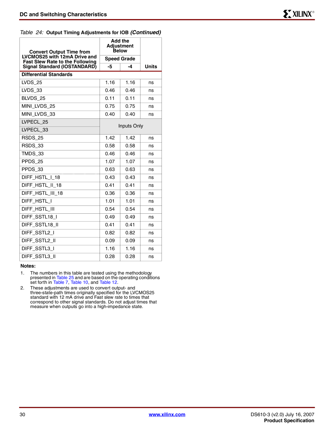
Table 24: Output Timing Adjustments for IOB (Continued)
| Add the |
|
| ||
| Adjustment |
|
| ||
Convert Output Time from | Below |
|
| ||
LVCMOS25 with 12mA Drive and |
|
|
|
|
|
Speed Grade |
|
| |||
Fast Slew Rate to the Following |
|
| |||
|
|
|
|
| |
Signal Standard (IOSTANDARD) |
|
| Units | ||
Differential Standards |
|
|
|
|
|
|
|
|
|
|
|
LVDS_25 | 1.16 |
| 1.16 |
| ns |
|
|
|
|
|
|
LVDS_33 | 0.46 |
| 0.46 |
| ns |
|
|
|
|
|
|
BLVDS_25 | 0.11 |
| 0.11 |
| ns |
|
|
|
|
|
|
MINI_LVDS_25 | 0.75 |
| 0.75 |
| ns |
|
|
|
|
|
|
MINI_LVDS_33 | 0.40 |
| 0.40 |
| ns |
|
|
|
|
|
|
LVPECL_25 |
| Inputs Only |
| ||
|
|
| |||
LVPECL_33 |
|
| |||
|
|
|
|
| |
|
|
|
|
|
|
RSDS_25 | 1.42 |
| 1.42 |
| ns |
|
|
|
|
|
|
RSDS_33 | 0.58 |
| 0.58 |
| ns |
|
|
|
|
|
|
TMDS_33 | 0.46 |
| 0.46 |
| ns |
|
|
|
|
|
|
PPDS_25 | 1.07 |
| 1.07 |
| ns |
|
|
|
|
|
|
PPDS_33 | 0.63 |
| 0.63 |
| ns |
|
|
|
|
|
|
DIFF_HSTL_I_18 | 0.43 |
| 0.43 |
| ns |
|
|
|
|
|
|
DIFF_HSTL_II_18 | 0.41 |
| 0.41 |
| ns |
|
|
|
|
|
|
DIFF_HSTL_III_18 | 0.36 |
| 0.36 |
| ns |
|
|
|
|
|
|
DIFF_HSTL_I | 1.01 |
| 1.01 |
| ns |
|
|
|
|
|
|
DIFF_HSTL_III | 0.54 |
| 0.54 |
| ns |
|
|
|
|
|
|
DIFF_SSTL18_I | 0.49 |
| 0.49 |
| ns |
|
|
|
|
|
|
DIFF_SSTL18_II | 0.41 |
| 0.41 |
| ns |
|
|
|
|
|
|
DIFF_SSTL2_I | 0.82 |
| 0.82 |
| ns |
|
|
|
|
|
|
DIFF_SSTL2_II | 0.09 |
| 0.09 |
| ns |
|
|
|
|
|
|
DIFF_SSTL3_I | 1.16 |
| 1.16 |
| ns |
|
|
|
|
|
|
DIFF_SSTL3_II | 0.28 |
| 0.28 |
| ns |
|
|
|
|
|
|
Notes:
1.The numbers in this table are tested using the methodology presented in Table 25 and are based on the operating conditions set forth in Table 7, Table 10, and Table 12.
2.These adjustments are used to convert output- and
R
30 | www.xilinx.com | |
|
| Product Specification |