R
DC and Switching Characteristics
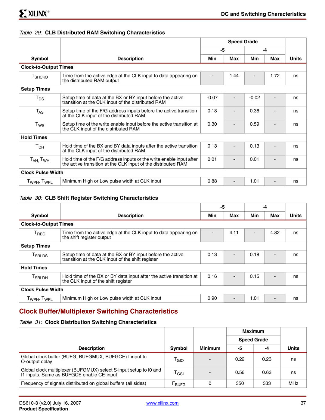
Table 29: CLB Distributed RAM Switching Characteristics
|
|
| Speed Grade |
|
|
| |
|
|
|
|
|
|
|
|
|
|
|
|
| |||
|
|
|
|
|
|
|
|
Symbol | Description | Min | Max | Min |
| Max | Units |
|
|
|
|
|
| ||
|
|
|
|
|
|
|
|
TSHCKO | Time from the active edge at the CLK input to data appearing on | - | 1.44 | - |
| 1.72 | ns |
| the distributed RAM output |
|
|
|
|
|
|
Setup Times |
|
|
|
|
|
|
|
|
|
|
|
|
|
|
|
TDS | Setup time of data at the BX or BY input before the active | - |
| - | ns | ||
| transition at the CLK input of the distributed RAM |
|
|
|
|
|
|
TAS | Setup time of the F/G address inputs before the active transition | 0.18 | - | 0.36 |
| - | ns |
| at the CLK input of the distributed RAM |
|
|
|
|
|
|
TWS | Setup time of the write enable input before the active transition at | 0.30 | - | 0.59 |
| - | ns |
| the CLK input of the distributed RAM |
|
|
|
|
|
|
Hold Times |
|
|
|
|
|
|
|
|
|
|
|
|
|
|
|
TDH | Hold time of the BX and BY data inputs after the active transition | 0.13 | - | 0.13 |
| - | ns |
| at the CLK input of the distributed RAM |
|
|
|
|
|
|
TAH, TWH | Hold time of the F/G address inputs or the write enable input after | 0.01 | - | 0.01 |
| - | ns |
| the active transition at the CLK input of the distributed RAM |
|
|
|
|
|
|
Clock Pulse Width |
|
|
|
|
|
| |
|
|
|
|
|
|
|
|
TWPH, TWPL | Minimum High or Low pulse width at CLK input | 0.88 | - | 1.01 |
| - | ns |
Table 30: CLB Shift Register Switching Characteristics
|
|
|
|
| ||||
|
|
|
|
|
|
|
|
|
Symbol | Description | Min |
| Max | Min |
| Max | Units |
|
|
|
|
|
|
| ||
|
|
|
|
|
|
|
|
|
TREG | Time from the active edge at the CLK input to data appearing on | - |
| 4.11 | - |
| 4.82 | ns |
| the shift register output |
|
|
|
|
|
|
|
Setup Times |
|
|
|
|
|
|
|
|
|
|
|
|
|
|
|
|
|
TSRLDS | Setup time of data at the BX or BY input before the active | 0.13 |
| - | 0.18 |
| - | ns |
| transition at the CLK input of the shift register |
|
|
|
|
|
|
|
Hold Times |
|
|
|
|
|
|
|
|
|
|
|
|
|
|
|
|
|
TSRLDH | Hold time of the BX or BY data input after the active transition at | 0.16 |
| - | 0.15 |
| - | ns |
| the CLK input of the shift register |
|
|
|
|
|
|
|
Clock Pulse Width |
|
|
|
|
|
|
| |
|
|
|
|
|
|
|
|
|
TWPH, TWPL | Minimum High or Low pulse width at CLK input | 0.90 |
| - | 1.01 |
| - | ns |
Clock Buffer/Multiplexer Switching Characteristics
Table 31: Clock Distribution Switching Characteristics
|
|
|
| Maximum |
| |
|
|
|
|
|
| |
|
|
|
| Speed Grade |
| |
|
|
|
|
|
|
|
Description |
| Symbol | Minimum | Units | ||
Global clock buffer (BUFG, BUFGMUX, BUFGCE) I input to | TGIO | - | 0.22 | 0.23 | ns | |
| ||||||
Global clock multiplexer (BUFGMUX) select | TGSI | - | 0.56 | 0.63 | ns | |
I1 inputs. Same as BUFGCE enable |
| |||||
Frequency of signals distributed on global buffers (all sides) |
| FBUFG | 0 | 350 | 333 | MHz |
|
|
|
|
|
|
|
www.xilinx.com |
|
|
| 37 | ||
Product Specification |
|
|
|
|
|
|