R
DC and Switching Characteristics
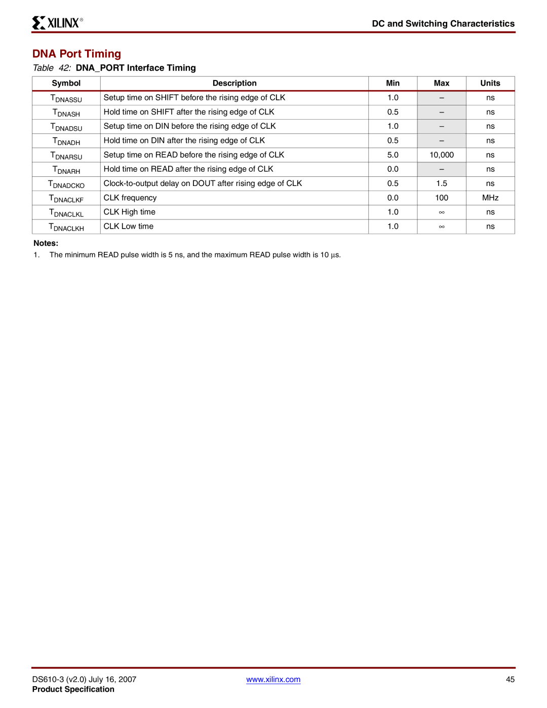
DNA Port Timing
Table 42: DNA_PORT Interface Timing
Symbol | Description | Min | Max | Units |
TDNASSU | Setup time on SHIFT before the rising edge of CLK | 1.0 | – | ns |
TDNASH | Hold time on SHIFT after the rising edge of CLK | 0.5 | – | ns |
TDNADSU | Setup time on DIN before the rising edge of CLK | 1.0 | – | ns |
TDNADH | Hold time on DIN after the rising edge of CLK | 0.5 | – | ns |
TDNARSU | Setup time on READ before the rising edge of CLK | 5.0 | 10,000 | ns |
TDNARH | Hold time on READ after the rising edge of CLK | 0.0 | – | ns |
TDNADCKO | 0.5 | 1.5 | ns | |
TDNACLKF | CLK frequency | 0.0 | 100 | MHz |
TDNACLKL | CLK High time | 1.0 | ∞ | ns |
TDNACLKH | CLK Low time | 1.0 | ∞ | ns |
Notes:
1.The minimum READ pulse width is 5 ns, and the maximum READ pulse width is 10 μs.
www.xilinx.com | 45 |
Product Specification