DC and Switching Characteristics
R
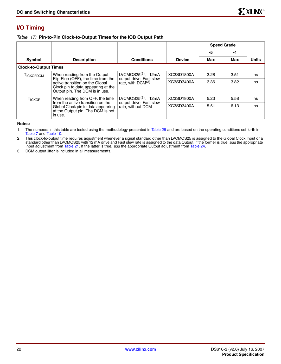
I/O Timing
Table 17: Pin-to-Pin Clock-to-Output Times for the IOB Output Path
|
|
|
| Speed Grade |
| |
|
|
|
|
|
|
|
|
|
|
|
| ||
|
|
|
|
|
|
|
Symbol | Description | Conditions | Device | Max | Max | Units |
|
|
|
|
| ||
|
|
|
|
|
|
|
TICKOFDCM | When reading from the Output | LVCMOS25(2), 12mA | XC3SD1800A | 3.28 | 3.51 | ns |
| output drive, Fast slew |
|
|
|
| |
| XC3SD3400A | 3.36 | 3.82 | ns | ||
| active transition on the Global | rate, with DCM(3) | ||||
| Clock pin to data appearing at the |
|
|
|
|
|
| Output pin. The DCM is in use. |
|
|
|
|
|
|
|
|
|
|
|
|
TICKOF | When reading from OFF, the time | LVCMOS25(2), 12mA | XC3SD1800A | 5.23 | 5.58 | ns |
| from the active transition on the | output drive, Fast slew |
|
|
|
|
| XC3SD3400A | 5.51 | 6.13 | ns | ||
| Global Clock pin to data appearing | rate, without DCM | ||||
| at the Output pin. The DCM is not |
|
|
|
|
|
| in use. |
|
|
|
|
|
|
|
|
|
|
|
|
Notes:
1.The numbers in this table are tested using the methodology presented in Table 25 and are based on the operating conditions set forth in Table 7 and Table 10.
2.This
3.DCM output jitter is included in all measurements.
22 | www.xilinx.com | |
|
| Product Specification |