R
DC and Switching Characteristics
Configuration and JTAG Timing
General Configuration Power-On/Reconfigure Timing
VCCINT
(Supply)
VCCAUX
(Supply)
VCCO Bank 2
(Supply)
PROG_B
(Input)
INIT_B
CCLK
(Output)
Notes:
1.0V
2.0V
1.0V
TPOR
TPROGTPL
TICCK
1.2V
2.5V or
3.3V
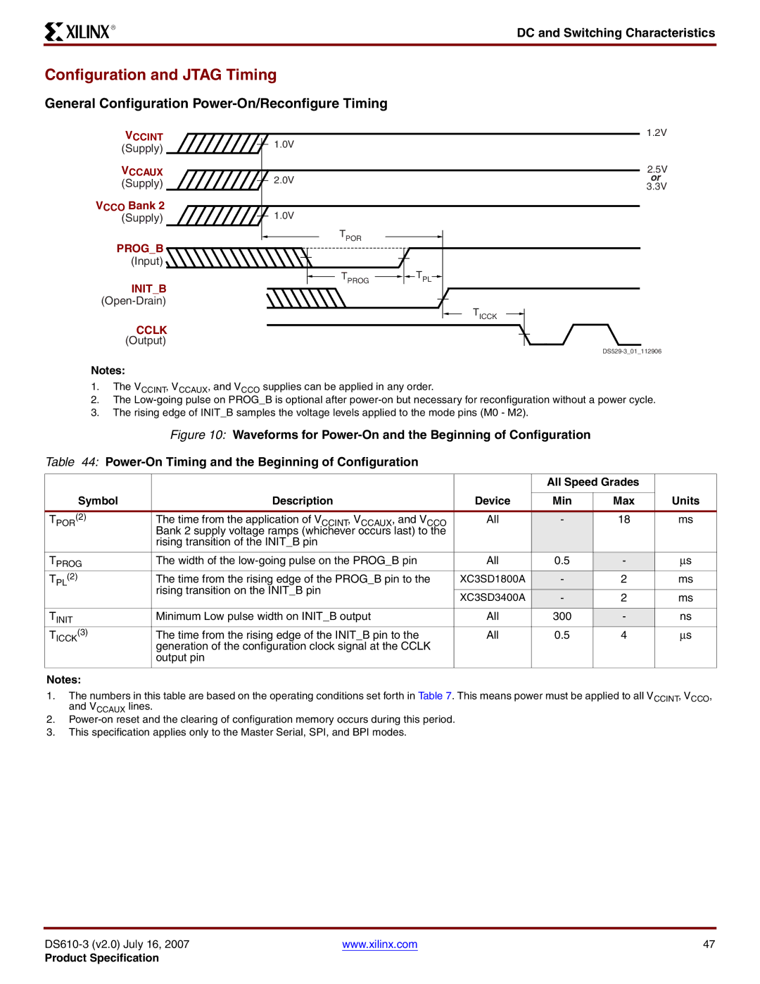
1.The VCCINT, VCCAUX, and VCCO supplies can be applied in any order.
2.The
3.The rising edge of INIT_B samples the voltage levels applied to the mode pins (M0 - M2).
Figure 10: Waveforms for Power-On and the Beginning of Configuration
Table 44: Power-On Timing and the Beginning of Configuration
|
|
| All Speed Grades |
| |
|
|
|
|
|
|
Symbol | Description | Device | Min | Max | Units |
TPOR(2) | The time from the application of VCCINT, VCCAUX, and VCCO | All | - | 18 | ms |
| Bank 2 supply voltage ramps (whichever occurs last) to the |
|
|
|
|
| rising transition of the INIT_B pin |
|
|
|
|
TPROG | The width of the | All | 0.5 | - | μs |
TPL(2) | The time from the rising edge of the PROG_B pin to the | XC3SD1800A | - | 2 | ms |
| rising transition on the INIT_B pin |
|
|
|
|
| XC3SD3400A | - | 2 | ms | |
|
| ||||
|
|
|
|
|
|
TINIT | Minimum Low pulse width on INIT_B output | All | 300 | - | ns |
TICCK(3) | The time from the rising edge of the INIT_B pin to the | All | 0.5 | 4 | μs |
| generation of the configuration clock signal at the CCLK |
|
|
|
|
| output pin |
|
|
|
|
|
|
|
|
|
|
Notes: |
|
|
|
|
|
1.The numbers in this table are based on the operating conditions set forth in Table 7. This means power must be applied to all VCCINT, VCCO, and VCCAUX lines.
2.
3.This specification applies only to the Master Serial, SPI, and BPI modes.
www.xilinx.com | 47 |
Product Specification
