R
DC and Switching Characteristics
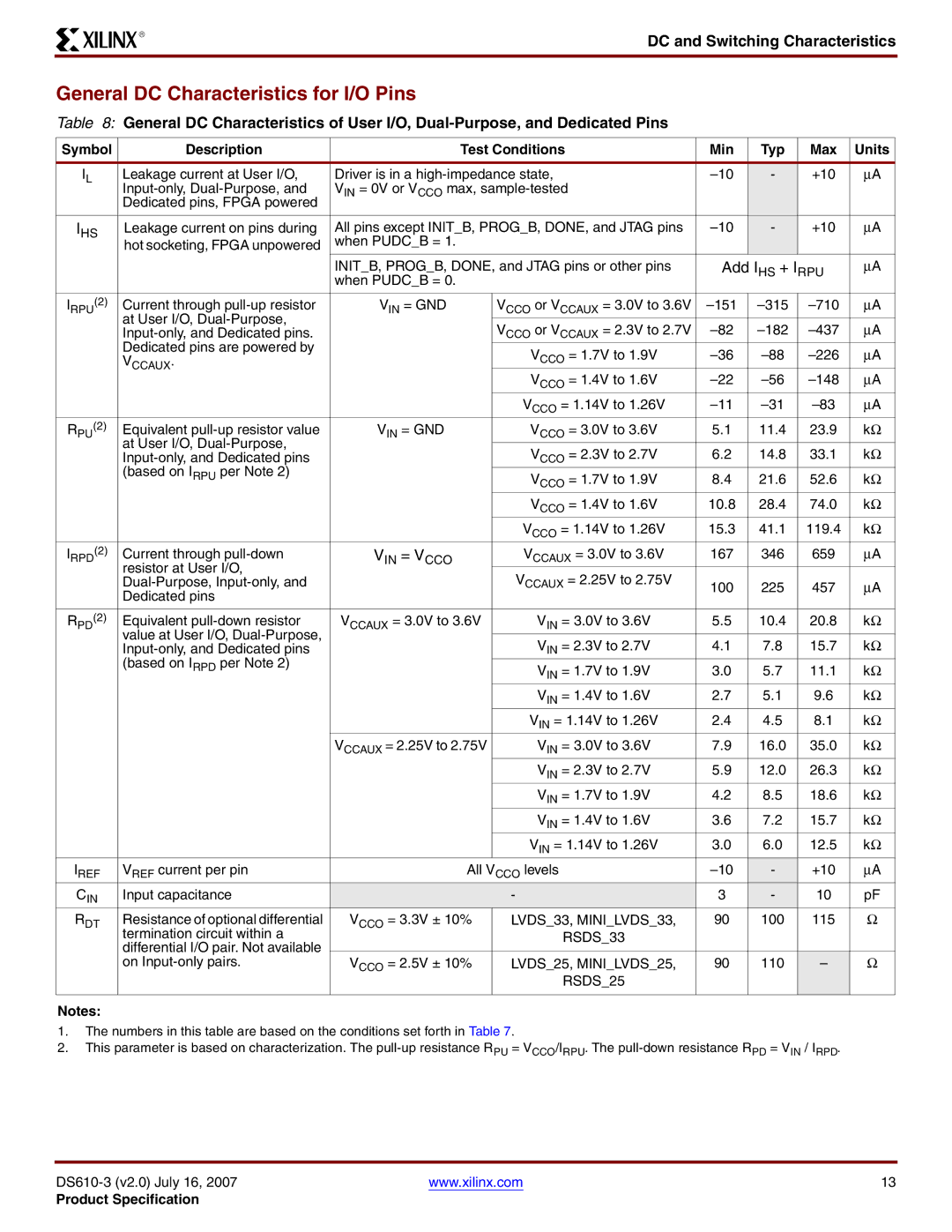
General DC Characteristics for I/O Pins
Table 8: General DC Characteristics of User I/O,
Symbol | Description | Test Conditions | Min | Typ | Max | Units | |
IL | Leakage current at User I/O, | Driver is in a | - | +10 | μA | ||
| VIN = 0V or VCCO max, |
|
|
|
| ||
| Dedicated pins, FPGA powered |
|
|
|
|
|
|
IHS | Leakage current on pins during | All pins except INIT_B, PROG_B, DONE, and JTAG pins | - | +10 | μA | ||
| hot socketing, FPGA unpowered | when PUDC_B = 1. |
|
|
|
|
|
|
| INIT_B, PROG_B, DONE, and JTAG pins or other pins | Add IHS + IRPU | μA | |||
|
| when PUDC_B = 0. |
|
|
|
|
|
IRPU(2) | Current through | VIN = GND | VCCO or VCCAUX = 3.0V to 3.6V | μA | |||
| at User I/O, |
|
|
|
|
|
|
|
| VCCO or VCCAUX = 2.3V to 2.7V | μA | ||||
|
| ||||||
| Dedicated pins are powered by |
|
|
|
|
|
|
|
| VCCO = 1.7V to 1.9V | μA | ||||
| VCCAUX. |
| |||||
|
| VCCO = 1.4V to 1.6V | μA | ||||
|
|
| |||||
|
|
| VCCO = 1.14V to 1.26V | μA | |||
RPU(2) | Equivalent | VIN = GND | VCCO = 3.0V to 3.6V | 5.1 | 11.4 | 23.9 | kΩ |
| at User I/O, |
|
|
|
|
|
|
|
| VCCO = 2.3V to 2.7V | 6.2 | 14.8 | 33.1 | kΩ | |
|
| ||||||
| (based on IRPU per Note 2) |
|
|
|
|
|
|
|
| VCCO = 1.7V to 1.9V | 8.4 | 21.6 | 52.6 | kΩ | |
|
|
| |||||
|
|
| VCCO = 1.4V to 1.6V | 10.8 | 28.4 | 74.0 | kΩ |
|
|
| VCCO = 1.14V to 1.26V | 15.3 | 41.1 | 119.4 | kΩ |
IRPD(2) | Current through | VIN = VCCO | VCCAUX = 3.0V to 3.6V | 167 | 346 | 659 | μA |
| resistor at User I/O, |
|
|
|
|
|
|
|
| VCCAUX = 2.25V to 2.75V |
|
|
|
| |
|
| 100 | 225 | 457 | μA | ||
| Dedicated pins |
|
| ||||
|
|
|
|
|
|
| |
|
|
|
|
|
|
|
|
RPD(2) | Equivalent | VCCAUX = 3.0V to 3.6V | VIN = 3.0V to 3.6V | 5.5 | 10.4 | 20.8 | kΩ |
| value at User I/O, |
|
|
|
|
|
|
|
| VIN = 2.3V to 2.7V | 4.1 | 7.8 | 15.7 | kΩ | |
|
| ||||||
| (based on IRPD per Note 2) |
|
|
|
|
|
|
|
| VIN = 1.7V to 1.9V | 3.0 | 5.7 | 11.1 | kΩ | |
|
|
| |||||
|
|
| VIN = 1.4V to 1.6V | 2.7 | 5.1 | 9.6 | kΩ |
|
|
| VIN = 1.14V to 1.26V | 2.4 | 4.5 | 8.1 | kΩ |
|
| VCCAUX = 2.25V to 2.75V | VIN = 3.0V to 3.6V | 7.9 | 16.0 | 35.0 | kΩ |
|
|
| VIN = 2.3V to 2.7V | 5.9 | 12.0 | 26.3 | kΩ |
|
|
| VIN = 1.7V to 1.9V | 4.2 | 8.5 | 18.6 | kΩ |
|
|
| VIN = 1.4V to 1.6V | 3.6 | 7.2 | 15.7 | kΩ |
|
|
| VIN = 1.14V to 1.26V | 3.0 | 6.0 | 12.5 | kΩ |
IREF | VREF current per pin | All VCCO levels | - | +10 | μA | ||
CIN | Input capacitance |
| - | 3 | - | 10 | pF |
RDT | Resistance of optional differential | VCCO = 3.3V ± 10% | LVDS_33, MINI_LVDS_33, | 90 | 100 | 115 | Ω |
| termination circuit within a |
| RSDS_33 |
|
|
|
|
| differential I/O pair. Not available |
|
|
|
|
|
|
| on | VCCO = 2.5V ± 10% | LVDS_25, MINI_LVDS_25, | 90 | 110 | – | Ω |
|
|
| RSDS_25 |
|
|
|
|
|
|
|
|
|
|
|
|
Notes:
1.The numbers in this table are based on the conditions set forth in Table 7.
2.This parameter is based on characterization. The
www.xilinx.com | 13 |
Product Specification