R
DC and Switching Characteristics
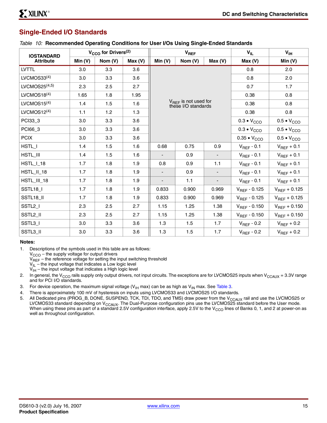
Single-Ended I/O Standards
Table 10: Recommended Operating Conditions for User I/Os Using
IOSTANDARD | VCCO for Drivers(2) |
|
| VREF |
| VIL | VIH | ||
Attribute | Min (V) | Nom (V) | Max (V) |
| Min (V) | Nom (V) | Max (V) | Max (V) | Min (V) |
LVTTL | 3.0 | 3.3 | 3.6 |
|
|
|
| 0.8 | 2.0 |
|
|
|
|
|
|
|
|
|
|
LVCMOS33(4) | 3.0 | 3.3 | 3.6 |
|
|
|
| 0.8 | 2.0 |
LVCMOS25(4,5) | 2.3 | 2.5 | 2.7 |
|
|
|
| 0.7 | 1.7 |
LVCMOS18(4) | 1.65 | 1.8 | 1.95 |
|
|
|
| 0.38 | 0.8 |
|
|
|
|
| VREF is not used for |
|
| ||
(4) | 1.4 | 1.5 | 1.6 |
| 0.38 | 0.8 | |||
LVCMOS15 |
| these I/O standards | |||||||
LVCMOS12(4) | 1.1 | 1.2 | 1.3 |
|
|
|
| 0.38 | 0.8 |
PCI33_3 | 3.0 | 3.3 | 3.6 |
|
|
|
| 0.3 • VCCO | 0.5 • VCCO |
PCI66_3 | 3.0 | 3.3 | 3.6 |
|
|
|
| 0.3 • VCCO | 0.5 • VCCO |
PCIX | 3.0 | 3.3 | 3.6 |
|
|
|
| 0.35 • VCCO | 0.5 • VCCO |
HSTL_I | 1.4 | 1.5 | 1.6 |
| 0.68 | 0.75 | 0.9 | VREF - 0.1 | VREF + 0.1 |
HSTL_III | 1.4 | 1.5 | 1.6 |
| - | 0.9 | - | VREF - 0.1 | VREF + 0.1 |
HSTL_I_18 | 1.7 | 1.8 | 1.9 |
| 0.8 | 0.9 | 1.1 | VREF - 0.1 | VREF + 0.1 |
HSTL_II_18 | 1.7 | 1.8 | 1.9 |
| - | 0.9 | - | VREF - 0.1 | VREF + 0.1 |
HSTL_III_18 | 1.7 | 1.8 | 1.9 |
| - | 1.1 | - | VREF - 0.1 | VREF + 0.1 |
SSTL18_I | 1.7 | 1.8 | 1.9 |
| 0.833 | 0.900 | 0.969 | VREF - 0.125 | VREF + 0.125 |
SSTL18_II | 1.7 | 1.8 | 1.9 |
| 0.833 | 0.900 | 0.969 | VREF - 0.125 | VREF + 0.125 |
SSTL2_I | 2.3 | 2.5 | 2.7 |
| 1.15 | 1.25 | 1.38 | VREF - 0.150 | VREF + 0.150 |
SSTL2_II | 2.3 | 2.5 | 2.7 |
| 1.15 | 1.25 | 1.38 | VREF - 0.150 | VREF + 0.150 |
SSTL3_I | 3.0 | 3.3 | 3.6 |
| 1.3 | 1.5 | 1.7 | VREF - 0.2 | VREF + 0.2 |
SSTL3_II | 3.0 | 3.3 | 3.6 |
| 1.3 | 1.5 | 1.7 | VREF - 0.2 | VREF + 0.2 |
Notes:
1.Descriptions of the symbols used in this table are as follows:
VCCO – the supply voltage for output drivers
VREF – the reference voltage for setting the input switching threshold VIL – the input voltage that indicates a Low logic level
VIH – the input voltage that indicates a High logic level
2.In general, the VCCO rails supply only output drivers, not input circuits. The exceptions are for LVCMOS25 inputs when VCCAUX = 3.3V range and for PCI I/O standards.
3.For device operation, the maximum signal voltage (VIH max) can be as high as VIN max. See Table 3.
4.There is approximately 100 mV of hysteresis on inputs using LVCMOS33 and LVCMOS25 I/O standards.
5.All Dedicated pins (PROG_B, DONE, SUSPEND, TCK, TDI, TDO, and TMS) draw power from the VCCAUX rail and use the LVCMOS25 or LVCMOS33 standard depending on VCCAUX. The
www.xilinx.com | 15 |
Product Specification