DC and Switching Characteristics
R
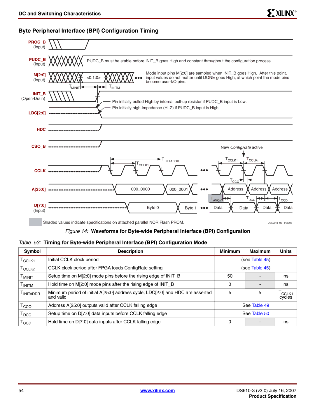
Byte Peripheral Interface (BPI) Configuration Timing
PROG_B
(Input)
PUDC_B
(Input)
M[2:0]
(Input)
INIT_B
LDC[2:0]
PUDC_B must be stable before INIT_B goes High and constant throughout the configuration process.
<0:1:0> | Mode input pins M[2:0] are sampled when INIT_B goes High. After this point, |
input values do not matter until DONE goes High, at which point the mode pins | |
| become |
TMINIT | TINITM |
![]() Pin initially pulled High by internal
Pin initially pulled High by internal
![]() Pin initially
Pin initially
HDC ![]()
CSO_B ![]()
TCCLK1
CCLK 
A[25:0] ![]() 000_0000
000_0000
D[7:0] | Byte 0 | |
(Input) | ||
|
TINITADDR
000_0001
Byte 1
New ConfigRate active
TCCLK1 TCCLKn
| TCCO |
|
|
| Address | Address | Address |
TAVQV | TDCC | TCCD | |
Data | Data | Data | Data |
![]() Shaded values indicate specifications on attached parallel NOR Flash PROM.
Shaded values indicate specifications on attached parallel NOR Flash PROM.
Figure 14: Waveforms for Byte-wide Peripheral Interface (BPI) Configuration
Table 53: | Timing for |
|
|
|
| |
|
|
|
|
|
|
|
Symbol |
| Description | Minimum |
| Maximum | Units |
TCCLK1 |
| Initial CCLK clock period |
| (see Table 45) |
| |
TCCLKn |
| CCLK clock period after FPGA loads ConfigRate setting |
| (see Table 45) |
| |
TMINIT |
| Setup time on M[2:0] mode pins before the rising edge of INIT_B | 50 |
| - | ns |
TINITM |
| Hold time on M[2:0] mode pins after the rising edge of INIT_B | 0 |
| - | ns |
TINITADDR |
| Minimum period of initial A[25:0] address cycle; LDC[2:0] and HDC are asserted | 5 |
| 5 | TCCLK1 |
|
| and valid |
|
|
| cycles |
|
|
|
|
|
|
|
TCCO |
| Address A[25:0] outputs valid after CCLK falling edge |
| See Table 49 |
| |
TDCC |
| Setup time on D[7:0] data inputs before CCLK falling edge |
| See Table 50 |
| |
TCCD |
| Hold time on D[7:0] data inputs after CCLK falling edge | 0 |
| - | ns |
54 | www.xilinx.com | |
|
| Product Specification |