R
Spartan-3A DSP FPGA Family: Pinout Descriptions
Product Specification | |
|
|
Introduction
This section describes how the various pins on a
•UG331:
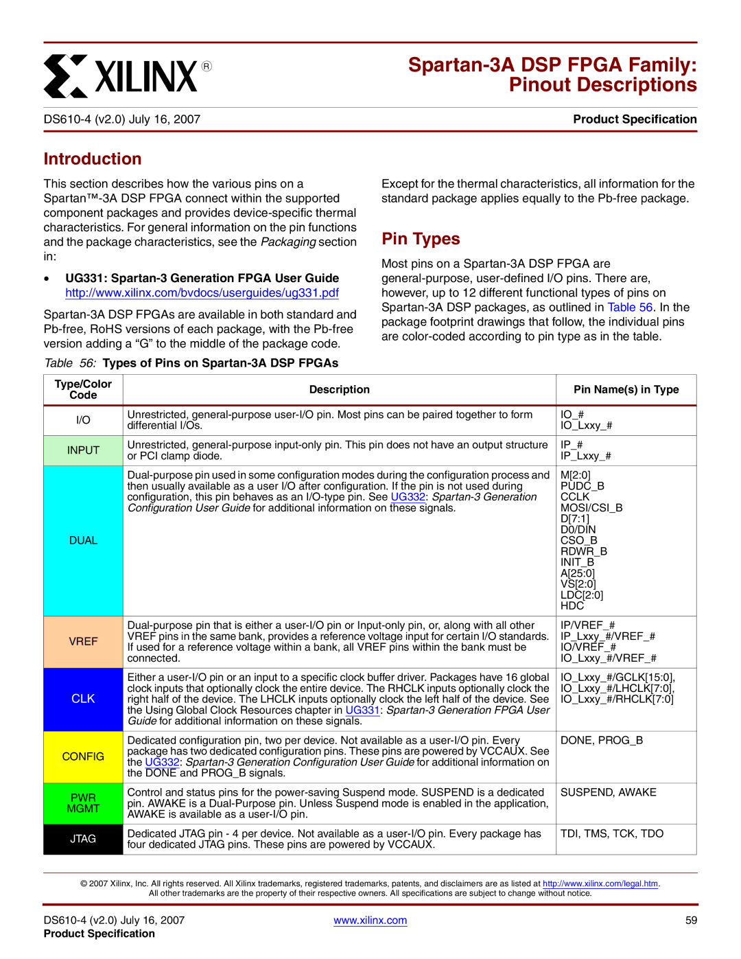
Table 56: Types of Pins on Spartan-3A DSP FPGAs
Except for the thermal characteristics, all information for the standard package applies equally to the
Pin Types
Most pins on a
Type/Color | Description | Pin Name(s) in Type | |
Code | |||
|
| ||
I/O | Unrestricted, | IO_# | |
differential I/Os. | IO_Lxxy_# | ||
| |||
|
|
| |
INPUT | Unrestricted, | IP_# | |
or PCI clamp diode. | IP_Lxxy_# | ||
| |||
| M[2:0] | ||
| then usually available as a user I/O after configuration. If the pin is not used during | PUDC_B | |
| configuration, this pin behaves as an | CCLK | |
| Configuration User Guide for additional information on these signals. | MOSI/CSI_B | |
|
| D[7:1] | |
|
| D0/DIN | |
DUAL |
| CSO_B | |
|
| RDWR_B | |
|
| INIT_B | |
|
| A[25:0] | |
|
| VS[2:0] | |
|
| LDC[2:0] | |
|
| HDC | |
| IP/VREF_# | ||
VREF | VREF pins in the same bank, provides a reference voltage input for certain I/O standards. | IP_Lxxy_#/VREF_# | |
If used for a reference voltage within a bank, all VREF pins within the bank must be | IO/VREF_# | ||
| |||
| connected. | IO_Lxxy_#/VREF_# | |
|
|
| |
| Either a | IO_Lxxy_#/GCLK[15:0], | |
CLK | clock inputs that optionally clock the entire device. The RHCLK inputs optionally clock the | IO_Lxxy_#/LHCLK[7:0], | |
right half of the device. The LHCLK inputs optionally clock the left half of the device. See | IO_Lxxy_#/RHCLK[7:0] | ||
| the Using Global Clock Resources chapter in UG331: |
| |
| Guide for additional information on these signals. |
| |
| Dedicated configuration pin, two per device. Not available as a | DONE, PROG_B | |
CONFIG | package has two dedicated configuration pins. These pins are powered by VCCAUX. See |
| |
the UG332: |
| ||
|
| ||
| the DONE and PROG_B signals. |
| |
|
|
| |
PWR | Control and status pins for the | SUSPEND, AWAKE | |
pin. AWAKE is a |
| ||
MGMT |
| ||
AWAKE is available as a |
| ||
|
| ||
|
|
| |
JTAG | Dedicated JTAG pin - 4 per device. Not available as a | TDI, TMS, TCK, TDO | |
four dedicated JTAG pins. These pins are powered by VCCAUX. |
| ||
|
| ||
|
|
|
© 2007 Xilinx, Inc. All rights reserved. All Xilinx trademarks, registered trademarks, patents, and disclaimers are as listed at http://www.xilinx.com/legal.htm.
All other trademarks are the property of their respective owners. All specifications are subject to change without notice.
www.xilinx.com | 59 |
Product Specification
