R
DC and Switching Characteristics
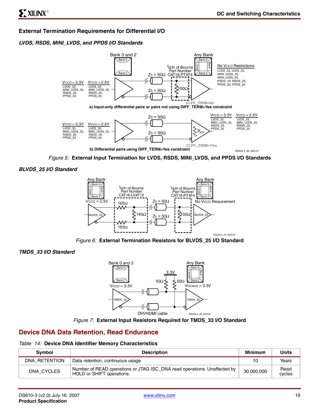
External Termination Requirements for Differential I/O
LVDS, RSDS, MINI_LVDS, and PPDS I/O Standards
Bank 0 and 2 |
Bank 0 |
Bank 2 |
VCCO = 3.3V VCCO = 2.5V
LVDS_33, LVDS_25,
MINI_LVDS_33, MINI_LVDS_25,
RSDS_33, RSDS_25,
PPDS_33 PPDS_25
|
| Any Bank | |
|
|
| Bank 0 |
| 1/4 th of Bourns | Bank 3 | Bank1 |
Z0 = 50Ω | Part Number |
| Bank 2 |
| |||
Z0 = 50Ω | 100Ω | ||||
| |||||
|
|
|
|
|
|
|
|
|
|
|
|
No VCCO Restrictions
LVDS_33, LVDS_25, MINI_LVDS_33, MINI_LVDS_25, RSDS_33, RSDS_25, PPDS_33, PPDS_25
DIFF_TERM=No
a)
Z0 = 50Ω |
VCCO = 3.3V VCCO = 2.5V
VCCO = 3.3V | VCCO = 2.5V |
|
|
|
|
|
|
|
|
| ||
|
|
|
|
|
|
|
|
| ||||
LVDS_33, | LVDS_25, |
|
|
|
|
|
|
|
|
| ||
MINI_LVDS_33, | MINI_LVDS_25, |
|
|
|
|
| Z0 = 50 |
| Ω | |||
|
|
|
|
| ||||||||
RSDS_33, | RSDS_25, |
|
|
|
| |||||||
PPDS_33 | PPDS_25 |
|
|
|
|
|
|
|
|
| ||
|
|
|
|
|
|
|
|
|
|
|
|
|
RDT
LVDS_33, LVDS_25,
MINI_LVDS_33, MINI_LVDS_25,
RSDS_33, RSDS_25,
PPDS_33 PPDS_25
DIFF_TERM=Yes |
|
b) Differential pairs using DIFF_TERM=Yes constraint | |
|
Figure 5: External Input Termination for LVDS, RSDS, MINI_LVDS, and PPDS I/O Standards
BLVDS_25 I/O Standard
Any Bank | Any Bank |
Bank 0 |
| 1/4 th of Bourns | 1/4 th of Bourns |
| Bank 0 | ||
3 | B | 3 | B | ||||
Bank | ank1 | Bank | ank1 | ||||
Part Number | Part Number |
| |||||
Bank 2 |
|
|
| Bank 2 | |||
VCCO = 2.5V | 165Ω | Z0 = 50Ω | No VCCO Requirement | ||||
|
|
|
|
|
| ||
BLVDS_25 | 140Ω | Z0 | = 50Ω | 100Ω BLVDS_25 |
|
|
|
165Ω
Figure 6: External Termination Resistors for BLVDS_25 I/O Standard
TMDS_33 I/O Standard
Bank 0 and 2 |
Bank 0 |
Bank 2 |
VCCO = 3.3V |
|
| Any Bank | |
|
|
| Bank 0 |
| 3.3V | 3 | B |
| Bank | ank 1 | |
50Ω |
| ||
| 50Ω | Bank 2 | |
|
|
| |
|
| VCCAUX = 3.3V | |
TMDS_33
TMDS_33
DVI/HDMI cableDS529-3_08_020107
Figure 7: External Input Resistors Required for TMDS_33 I/O Standard
Device DNA Data Retention, Read Endurance
Table 14: Device DNA Identifier Memory Characteristics
Symbol |
| Description | Minimum | Units |
DNA_RETENTION | Data retention, continuous usage |
| 10 | Years |
|
|
|
| |
DNA_CYCLES | Number of READ operations or JTAG ISC_DNA read operations. Unaffected by | 30,000,000 | Read | |
HOLD or SHIFT operations. |
| cycles | ||
|
|
| ||
|
|
|
|
|
|
|
|
|
|
www.xilinx.com |
| 19 | ||
Product Specification |
|
|
|
|