Pinout Descriptions
R
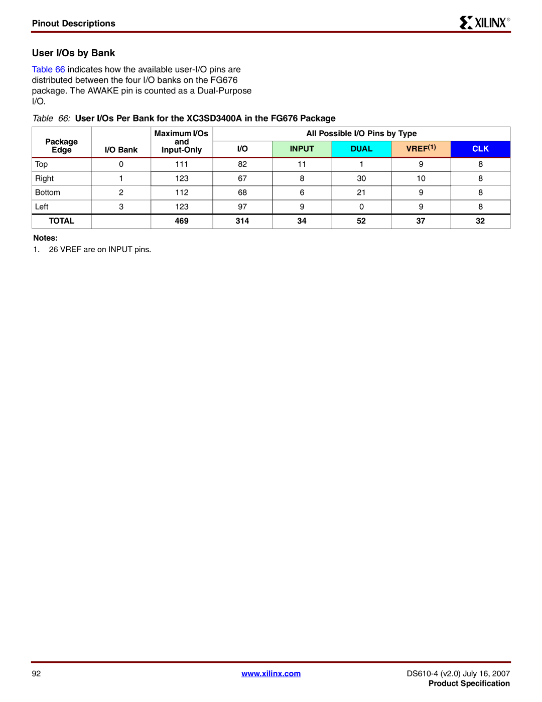
User I/Os by Bank
Table 66 indicates how the available
Table 66: User I/Os Per Bank for the XC3SD3400A in the FG676 Package
Package |
| Maximum I/Os |
| All Possible I/O Pins by Type |
| |||
| and |
|
|
|
|
| ||
I/O Bank | I/O | INPUT | DUAL | VREF(1) | CLK | |||
Edge |
| |||||||
Top | 0 | 111 | 82 | 11 | 1 | 9 | 8 | |
|
|
|
|
|
|
|
| |
Right | 1 | 123 | 67 | 8 | 30 | 10 | 8 | |
|
|
|
|
|
|
|
| |
Bottom | 2 | 112 | 68 | 6 | 21 | 9 | 8 | |
|
|
|
|
|
|
|
| |
Left | 3 | 123 | 97 | 9 | 0 | 9 | 8 | |
|
|
|
|
|
|
|
| |
TOTAL |
| 469 | 314 | 34 | 52 | 37 | 32 | |
|
|
|
|
|
|
|
| |
Notes:
1.26 VREF are on INPUT pins.
92 | www.xilinx.com | |
|
| Product Specification |