DC and Switching Characteristics
R
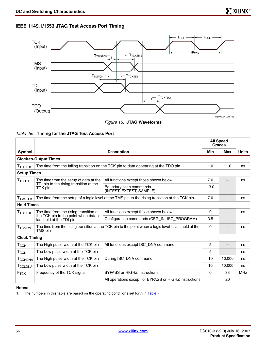
IEEE 1149.1/1553 JTAG Test Access Port Timing
TCK (Input)
TTMSTCK
TMS (Input)
TTDITCK
TDI (Input)
TDO (Output)
TCCH | TCCL |
TTCKTMS | 1/FTCK |
| |
TTCKTDI |
|
TTCKTDO |
|
| DS099_06_040703 |
Figure 15: JTAG Waveforms
Table 55: Timing for the JTAG Test Access Port
|
|
| All Speed |
| |
|
|
| Grades |
| |
|
|
|
|
|
|
Symbol |
| Description | Min | Max | Units |
|
|
|
| ||
|
|
|
|
|
|
TTCKTDO | The time from the falling transition on the TCK pin to data appearing at the TDO pin | 1.0 | 11.0 | ns | |
Setup Times |
|
|
|
| |
|
|
|
|
|
|
TTDITCK | The time from the setup of data at the | All functions except those shown below | 7.0 | – | ns |
| TDI pin to the rising transition at the |
|
|
|
|
| Boundary scan commands | 13.0 |
|
| |
| TCK pin |
|
| ||
|
| (INTEST, EXTEST, SAMPLE) |
|
|
|
TTMSTCK | The time from the setup of a logic level at the TMS pin to the rising transition at the TCK pin | 7.0 | – | ns | |
Hold Times |
|
|
|
| |
|
|
|
|
|
|
TTCKTDI | The time from the rising transition at | All functions except those shown below | 0 | – | ns |
| the TCK pin to the point when data is |
|
|
|
|
| Configuration commands (CFG_IN, ISC_PROGRAM) | 3.5 |
|
| |
| last held at the TDI pin |
|
| ||
|
|
|
|
|
|
TTCKTMS | The time from the rising transition at the TCK pin to the point when a logic level is last held at the | 0 | – | ns | |
| TMS pin |
|
|
|
|
Clock Timing |
|
|
|
| |
|
|
|
|
|
|
TCCH | The High pulse width at the TCK pin | All functions except ISC_DNA command | 5 | – | ns |
TCCL | The Low pulse width at the TCK pin |
| 5 | – | ns |
TCCHDNA | The High pulse width at the TCK pin | During ISC_DNA command | 10 | 10,000 | ns |
TCCLDNA | The Low pulse width at the TCK pin |
| 10 | 10,000 | ns |
FTCK | Frequency of the TCK signal | BYPASS or HIGHZ instructions | 0 | 33 | MHz |
|
| All operations except for BYPASS or HIGHZ instructions |
| 20 |
|
|
|
|
|
|
|
Notes:
1.The numbers in this table are based on the operating conditions set forth in Table 7.
56 | www.xilinx.com | |
|
| Product Specification |