DC and Switching Characteristics
R
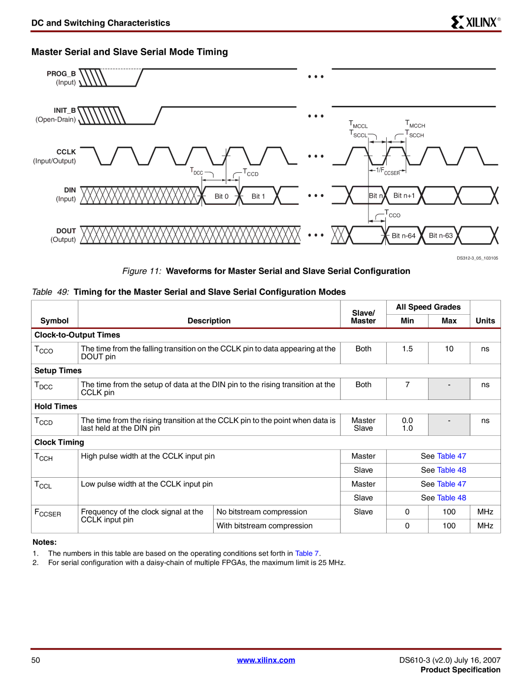
Master Serial and Slave Serial Mode Timing
PROG_B |
|
|
|
|
|
|
|
|
|
|
|
|
|
|
|
|
|
|
|
|
|
|
|
|
|
|
(Input) |
|
|
|
|
|
|
|
|
|
|
|
|
|
|
|
|
|
|
|
|
|
|
|
|
|
|
INIT_B |
|
|
|
|
|
|
|
|
|
|
|
|
|
|
|
|
|
|
|
|
|
|
|
|
|
|
|
|
|
|
|
|
|
|
|
|
|
|
|
|
|
|
|
|
|
|
|
|
|
|
|
| |
|
|
|
|
|
|
|
|
|
|
|
| TMCCL |
|
|
| TMCCH |
|
| ||||||||
|
|
|
|
|
|
|
|
|
|
|
|
|
|
|
|
|
| |||||||||
|
|
|
|
|
|
|
|
|
|
|
|
| TSCCL |
|
|
| TSCCH |
|
| |||||||
CCLK |
|
|
|
|
|
|
|
|
|
|
|
|
|
|
|
|
|
|
|
|
|
|
|
|
|
|
(Input/Output) |
|
|
|
|
|
|
|
|
|
|
|
|
|
|
|
|
|
|
|
|
|
|
|
|
|
|
DIN |
|
|
| TDCC |
|
|
| TCCD |
|
|
| 1/FCCSER |
|
|
|
| ||||||||||
|
|
|
|
|
|
|
| |||||||||||||||||||
|
|
|
|
| Bit 0 | Bit 1 | Bit n |
|
| Bit n+1 |
|
|
|
| ||||||||||||
(Input) |
|
|
|
|
|
|
|
|
|
|
| |||||||||||||||
|
|
|
|
|
|
|
|
|
|
|
|
|
|
|
|
|
|
|
|
|
|
|
|
|
| |
|
|
|
|
|
|
|
|
|
|
|
|
|
|
|
|
|
|
| TCCO |
|
|
|
| |||
DOUT |
|
|
|
|
|
|
|
|
|
|
|
|
|
|
|
|
|
|
|
| Bit |
| Bit |
|
| |
|
|
|
|
|
|
|
|
|
|
|
|
|
|
|
|
|
|
|
|
|
|
| ||||
(Output) |
|
|
|
|
|
|
|
|
|
|
|
|
|
|
|
|
|
|
|
|
|
|
| |||
|
|
|
|
|
|
|
|
|
|
|
|
|
|
|
|
|
|
|
|
|
|
|
|
|
| |
|
|
|
|
|
|
|
|
|
|
|
|
|
|
|
|
|
|
|
|
|
|
|
| |||
|
|
| Figure 11: Waveforms for Master Serial and Slave Serial Configuration |
|
|
|
| |||||||||||||||||||
Table 49: Timing for the Master Serial and Slave Serial Configuration Modes |
|
|
|
|
|
|
|
|
|
|
|
|
|
| ||||||||||||
|
|
|
|
|
|
|
|
|
|
|
|
|
|
|
|
|
|
|
|
|
|
|
|
|
| |
|
|
|
|
|
|
|
|
|
|
|
|
| Slave/ |
|
| All Speed Grades |
|
| ||||||||
|
|
|
|
|
|
|
|
|
|
|
|
|
|
|
|
|
|
|
|
| ||||||
Symbol |
|
|
| Description |
|
|
|
| Master |
|
| Min |
| Max | Units | |||||||||||
|
|
|
|
|
|
|
|
|
|
|
|
|
|
|
|
|
|
| ||||||||
|
|
|
|
|
|
|
|
|
|
|
|
|
|
|
|
|
|
|
|
|
|
|
|
|
| |
TCCO |
| The time from the falling transition on the CCLK pin to data appearing at the |
| Both |
| 1.5 |
| 10 | ns | |||||||||||||||||
|
| DOUT pin |
|
|
|
|
|
|
|
|
|
|
|
|
|
|
|
|
|
| ||||||
|
|
|
|
|
|
|
|
|
|
|
|
|
|
|
|
|
|
|
|
|
|
|
|
|
|
|
Setup Times |
|
|
|
|
|
|
|
|
|
|
|
|
|
|
|
|
|
| ||||||||
|
|
|
|
|
|
|
|
|
|
|
|
|
|
|
|
|
|
|
|
|
|
|
|
|
| |
TDCC |
| The time from the setup of data at the DIN pin to the rising transition at the |
| Both |
| 7 |
| - | ns | |||||||||||||||||
|
| CCLK pin |
|
|
|
|
|
|
|
|
|
|
|
|
|
|
|
|
|
| ||||||
Hold Times |
|
|
|
|
|
|
|
|
|
|
|
|
|
|
|
|
|
|
|
|
|
|
|
|
|
|
|
|
|
|
|
|
|
|
|
|
|
|
|
|
|
|
|
|
|
|
|
|
|
|
|
| |
TCCD |
| The time from the rising transition at the CCLK pin to the point when data is |
| Master |
| 0.0 |
| - | ns | |||||||||||||||||
|
| last held at the DIN pin |
|
|
|
| Slave |
| 1.0 |
|
|
|
| |||||||||||||
Clock Timing |
|
|
|
|
|
|
|
|
|
|
|
|
|
|
|
|
|
| ||||||||
|
|
|
|
|
|
|
|
|
|
|
|
|
|
|
|
|
|
|
|
|
|
|
|
|
|
|
TCCH |
| High pulse width at the CCLK input pin |
|
|
|
| Master |
|
|
|
| See Table 47 |
|
| ||||||||||||
|
|
|
|
|
|
|
|
|
|
|
|
| Slave |
|
|
|
| See Table 48 |
|
| ||||||
|
|
|
|
|
|
|
|
|
|
|
|
|
|
|
|
|
|
|
|
|
|
|
|
| ||
TCCL |
| Low pulse width at the CCLK input pin |
|
|
|
| Master |
|
|
|
| See Table 47 |
|
| ||||||||||||
|
|
|
|
|
|
|
|
|
|
|
|
| Slave |
|
|
|
| See Table 48 |
|
| ||||||
|
|
|
|
|
|
|
|
|
|
|
|
|
|
|
|
|
|
|
|
|
|
|
|
| ||
FCCSER |
| Frequency of the clock signal at the | No bitstream compression |
| Slave |
| 0 |
| 100 | MHz | ||||||||||||||||
|
| CCLK input pin |
|
|
|
|
|
|
|
|
|
|
|
|
|
|
|
|
|
|
|
|
| |||
| With bitstream compression |
|
|
|
|
|
|
|
| 0 |
| 100 | MHz | |||||||||||||
|
|
|
|
|
|
|
|
|
|
|
|
|
|
| ||||||||||||
|
|
|
|
|
|
|
|
|
|
|
|
|
|
|
|
|
|
|
|
|
|
|
|
|
|
|
Notes:
1.The numbers in this table are based on the operating conditions set forth in Table 7.
2.For serial configuration with a
50 | www.xilinx.com | |
|
| Product Specification |