R
DC and Switching Characteristics
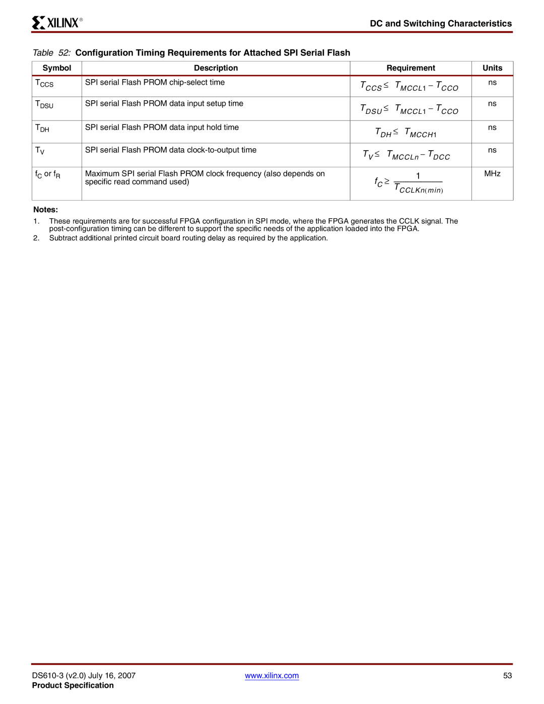
Table 52: Configuration Timing Requirements for Attached SPI Serial Flash
Symbol | Description |
| Requirement | Units |
TCCS | SPI serial Flash PROM | TCCS ≤ TM CC L1 – TCC O | ns | |
TDSU | SPI serial Flash PROM data input setup time | TDSU | ≤ TM CC L1 – TCC O | ns |
|
|
| ||
TDH | SPI serial Flash PROM data input hold time | TDH ≤ TMCCH1 | ns | |
|
|
| ||
TV | SPI serial Flash PROM data | TV ≤ | TMCC Ln – TD CC | ns |
|
|
| ||
fC or fR | Maximum SPI serial Flash PROM clock frequency (also depends on |
| 1 | MHz |
| specific read command used) | fC | ≥ |
|
|
|
| TCCL Kn(min) |
|
Notes:
1.These requirements are for successful FPGA configuration in SPI mode, where the FPGA generates the CCLK signal. The
2.Subtract additional printed circuit board routing delay as required by the application.
www.xilinx.com | 53 |
Product Specification