R
DC and Switching Characteristics
Timing Measurement Methodology
When measuring timing parameters at the programmable I/Os, different signal standards call for different test conditions. Table 25 lists the conditions to use for each standard.
open connection, and VT is set to zero. The same measurement point (VM) that was used at the Input is also used at the Output.
The method for measuring Input timing is as follows: A signal that swings between a Low logic level of VL and a High logic level of VH is applied to the Input under test. Some standards also require the application of a bias
voltage to the VREF pins of a given bank to properly set the
Input signal (VM) is commonly located halfway between VL and VH.
VT (VREF)
FPGA Output
RT (RREF)
![]() VM (VMEAS)
VM (VMEAS)
CL (CREF)
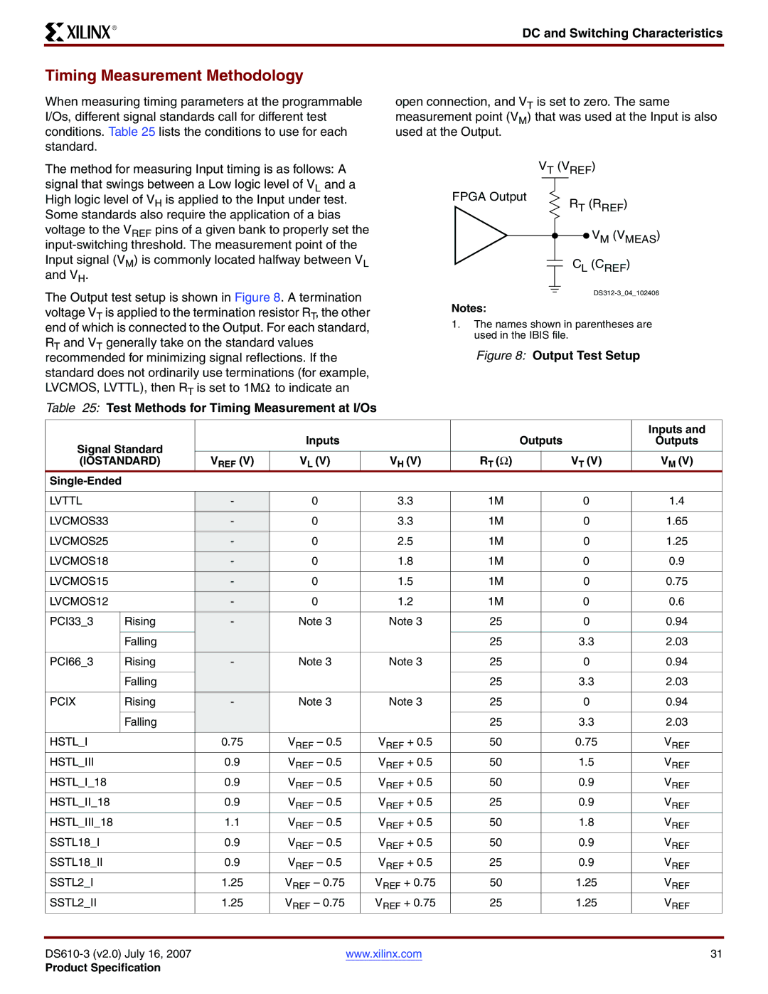
The Output test setup is shown in Figure 8. A termination voltage VT is applied to the termination resistor RT, the other end of which is connected to the Output. For each standard, RT and VT generally take on the standard values recommended for minimizing signal reflections. If the standard does not ordinarily use terminations (for example, LVCMOS, LVTTL), then RT is set to 1MΩ to indicate an
Table 25: Test Methods for Timing Measurement at I/Os
Notes:
1.The names shown in parentheses are used in the IBIS file.
Figure 8: Output Test Setup
|
|
|
|
|
|
|
|
|
|
| Inputs and |
Signal Standard |
|
| Inputs |
|
|
| Outputs | Outputs | |||
|
|
|
|
|
|
|
|
| |||
(IOSTANDARD) | VREF (V) | VL (V) |
| VH (V) | RT (Ω) |
| VT (V) | VM (V) | |||
|
|
|
|
|
|
|
|
|
|
| |
|
|
|
|
|
|
|
|
|
|
|
|
LVTTL |
|
| - | 0 |
| 3.3 | 1M |
| 0 | 1.4 | |
|
|
|
|
|
|
|
|
|
|
| |
LVCMOS33 |
|
| - | 0 |
| 3.3 | 1M |
| 0 | 1.65 | |
|
|
|
|
|
|
|
|
|
|
| |
LVCMOS25 |
|
| - | 0 |
| 2.5 | 1M |
| 0 | 1.25 | |
|
|
|
|
|
|
|
|
|
|
| |
LVCMOS18 |
|
| - | 0 |
| 1.8 | 1M |
| 0 | 0.9 | |
|
|
|
|
|
|
|
|
|
|
| |
LVCMOS15 |
|
| - | 0 |
| 1.5 | 1M |
| 0 | 0.75 | |
|
|
|
|
|
|
|
|
|
|
| |
LVCMOS12 |
|
| - | 0 |
| 1.2 | 1M |
| 0 | 0.6 | |
|
|
|
|
|
|
|
|
|
|
| |
PCI33_3 |
| Rising | - | Note 3 |
| Note 3 | 25 |
| 0 | 0.94 | |
|
|
|
|
|
|
|
|
|
|
| |
|
| Falling |
|
|
|
| 25 |
| 3.3 | 2.03 | |
|
|
|
|
|
|
|
|
|
|
| |
PCI66_3 |
| Rising | - | Note 3 |
| Note 3 | 25 |
| 0 | 0.94 | |
|
|
|
|
|
|
|
|
|
|
| |
|
| Falling |
|
|
|
| 25 |
| 3.3 | 2.03 | |
|
|
|
|
|
|
|
|
|
|
| |
PCIX |
| Rising | - | Note 3 |
| Note 3 | 25 |
| 0 | 0.94 | |
|
|
|
|
|
|
|
|
|
|
| |
|
| Falling |
|
|
|
| 25 |
| 3.3 | 2.03 | |
|
|
|
|
|
|
|
|
|
|
|
|
HSTL_I |
|
| 0.75 | VREF – 0.5 |
| VREF + 0.5 | 50 |
| 0.75 | VREF | |
HSTL_III |
|
| 0.9 | VREF – 0.5 |
| VREF + 0.5 | 50 |
| 1.5 | VREF | |
HSTL_I_18 |
|
| 0.9 | VREF – 0.5 |
| VREF + 0.5 | 50 |
| 0.9 | VREF | |
HSTL_II_18 |
|
| 0.9 | VREF – 0.5 |
| VREF + 0.5 | 25 |
| 0.9 | VREF | |
HSTL_III_18 |
|
| 1.1 | VREF – 0.5 |
| VREF + 0.5 | 50 |
| 1.8 | VREF | |
SSTL18_I |
|
| 0.9 | VREF – 0.5 |
| VREF + 0.5 | 50 |
| 0.9 | VREF | |
SSTL18_II |
|
| 0.9 | VREF – 0.5 |
| VREF + 0.5 | 25 |
| 0.9 | VREF | |
SSTL2_I |
|
| 1.25 | VREF – 0.75 |
| VREF + 0.75 | 50 |
| 1.25 | VREF | |
SSTL2_II |
|
| 1.25 | VREF – 0.75 |
| VREF + 0.75 | 25 |
| 1.25 | VREF | |
|
|
|
|
|
|
|
|
|
|
|
|
|
| www.xilinx.com |
|
|
| 31 | |||||
Product Specification |
|
|
|
|
|
|
|
| |||