R
DC and Switching Characteristics
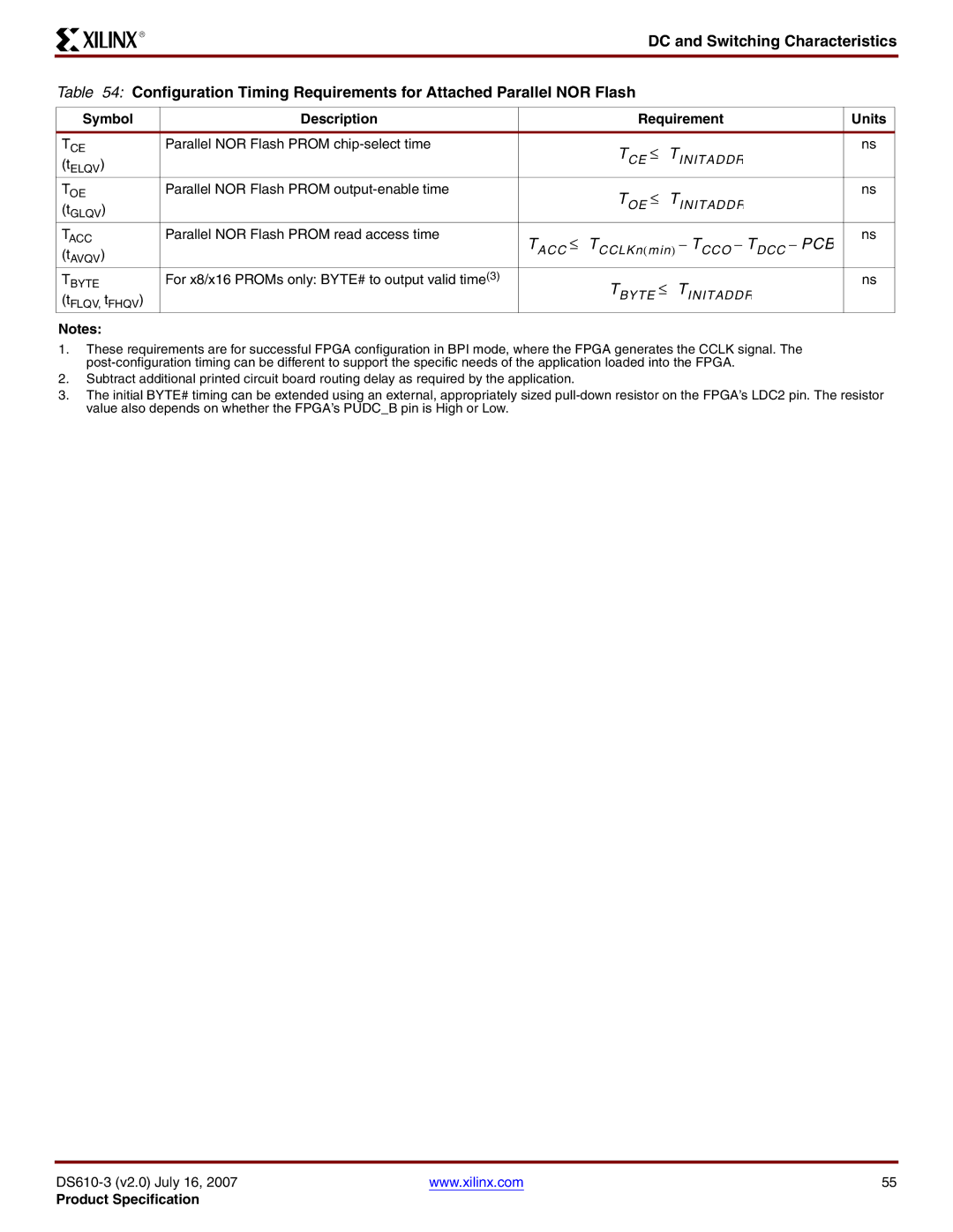
Table 54: Configuration Timing Requirements for Attached Parallel NOR Flash
Symbol | Description |
| Requirement |
| Units | |
TCE | Parallel NOR Flash PROM |
| TCE ≤ | TIN ITADDR |
| ns |
(tELQV) |
|
|
|
| ||
|
|
|
|
|
| |
TOE | Parallel NOR Flash PROM |
| TOE ≤ | TINITAD DR |
| ns |
(tGLQV) |
|
|
|
| ||
|
|
|
|
|
| |
TACC | Parallel NOR Flash PROM read access time | TACC | ≤ TCCL Kn(min) – TCC O – | TDCC – PCB | ns | |
(tAVQV) |
|
| ||||
|
|
|
|
|
| |
TBYTE | For x8/x16 PROMs only: BYTE# to output valid time(3) |
| TBYTE ≤ | TINITAD DR | ns | |
(tFLQV, tFHQV) |
|
|
| |||
|
|
|
|
|
| |
Notes:
1.These requirements are for successful FPGA configuration in BPI mode, where the FPGA generates the CCLK signal. The
2.Subtract additional printed circuit board routing delay as required by the application.
3.The initial BYTE# timing can be extended using an external, appropriately sized
www.xilinx.com | 55 |
Product Specification