DC and Switching Characteristics
R
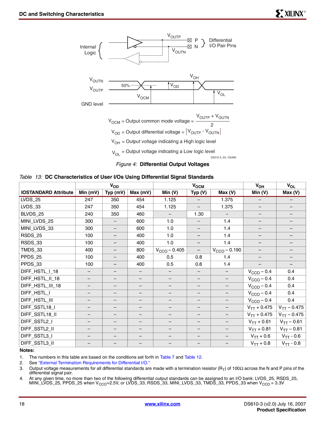
Internal
Logic
VOUTN
VOUTP
GND level
VOUTP
P | Differential |
N | I/O Pair Pins |
VOUTN
VOH
50% | VOD |
| VOL |
| VOCM |
VOCM
VOD
VOH
VOL
VOUTP + VOUTN
= Output common mode voltage =
2
=Output differential voltage = VOUTP - VOUTN
=Output voltage indicating a High logic level
=Output voltage indicating a Low logic level
Figure 4: Differential Output Voltages
Table 13: DC Characteristics of User I/Os Using Differential Signal Standards
|
| VOD |
|
| VOCM |
| VOH | VOL |
IOSTANDARD Attribute | Min (mV) | Typ (mV) | Max (mV) | Min (V) | Typ (V) | Max (V) | Min (V) | Max (V) |
LVDS_25 | 247 | 350 | 454 | 1.125 | – | 1.375 | – | – |
LVDS_33 | 247 | 350 | 454 | 1.125 | – | 1.375 | – | – |
BLVDS_25 | 240 | 350 | 460 | – | 1.30 | – | – | – |
MINI_LVDS_25 | 300 | – | 600 | 1.0 | – | 1.4 | – | – |
MINI_LVDS_33 | 300 | – | 600 | 1.0 | – | 1.4 | – | – |
RSDS_25 | 100 | – | 400 | 1.0 | – | 1.4 | – | – |
RSDS_33 | 100 | – | 400 | 1.0 | – | 1.4 | – | – |
TMDS_33 | 400 | – | 800 | VCCO – 0.405 | – | VCCO – 0.190 | – | – |
PPDS_25 | 100 | – | 400 | 0.5 | 0.8 | 1.4 | – | – |
PPDS_33 | 100 | – | 400 | 0.5 | 0.8 | 1.4 | – | – |
DIFF_HSTL_I_18 | – | – | – | – | – | – | VCCO – 0.4 | 0.4 |
DIFF_HSTL_II_18 | – | – | – | – | – | – | VCCO – 0.4 | 0.4 |
DIFF_HSTL_III_18 | – | – | – | – | – | – | VCCO – 0.4 | 0.4 |
DIFF_HSTL_I | – | – | – | – | – | – | VCCO – 0.4 | 0.4 |
DIFF_HSTL_III | – | – | – | – | – | – | VCCO – 0.4 | 0.4 |
DIFF_SSTL18_I | – | – | – | – | – | – | VTT + 0.475 | VTT – 0.475 |
DIFF_SSTL18_II | – | – | – | – | – | – | VTT + 0.475 | VTT – 0.475 |
DIFF_SSTL2_I | – | – | – | – | – | – | VTT + 0.61 | VTT – 0.61 |
DIFF_SSTL2_II | – | – | – | – | – | – | VTT + 0.81 | VTT – 0.81 |
DIFF_SSTL3_I | – | – | – | – | – | – | VTT + 0.6 | VTT - 0.6 |
DIFF_SSTL3_II | – | – | – | – | – | – | VTT + 0.8 | VTT - 0.8 |
Notes: |
|
|
|
|
|
|
|
|
1.The numbers in this table are based on the conditions set forth in Table 7 and Table 12.
2.See "External Termination Requirements for Differential I/O."
3.Output voltage measurements for all differential standards are made with a termination resistor (RT) of 100Ω across the N and P pins of the differential signal pair.
4.At any given time, no more than two of the following differential output standards can be assigned to an I/O bank: LVDS_25, RSDS_25, MINI_LVDS_25, PPDS_25 when VCCO=2.5V, or LVDS_33, RSDS_33, MINI_LVDS_33, TMDS_33, PPDS_33 when VCCO = 3.3V
18 | www.xilinx.com | |
|
| Product Specification |