DC and Switching Characteristics
R
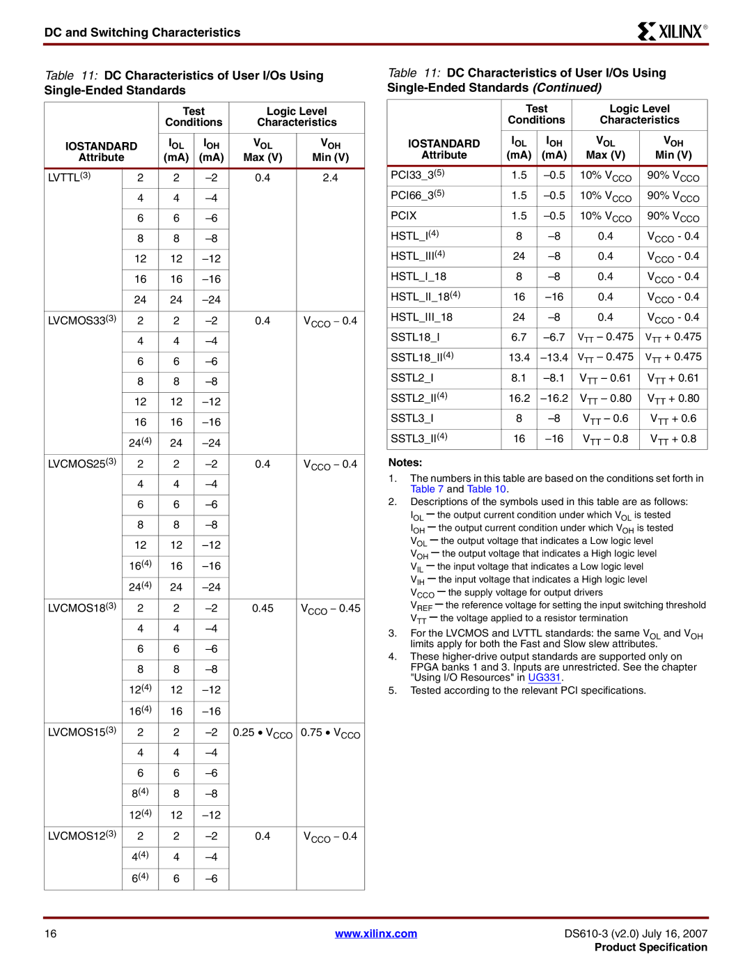
Table 11: DC Characteristics of User I/Os Using
|
|
| Test | Logic Level |
| |||
|
|
| Conditions | Characteristics | ||||
|
|
|
|
|
| |||
IOSTANDARD | IOL | IOH | VOL |
| VOH | |||
Attribute |
| (mA) | (mA) | Max (V) |
| Min (V) | ||
|
|
|
|
|
|
| ||
LVTTL(3) |
| 2 | 2 | 0.4 |
| 2.4 | ||
|
| 4 | 4 |
|
|
|
| |
|
|
|
|
|
|
|
|
|
|
| 6 | 6 |
|
|
|
| |
|
|
|
|
|
|
|
|
|
|
| 8 | 8 |
|
|
|
| |
|
|
|
|
|
|
|
|
|
|
| 12 | 12 |
|
|
|
| |
|
|
|
|
|
|
|
|
|
|
| 16 | 16 |
|
|
|
| |
|
|
|
|
|
|
|
|
|
|
| 24 | 24 |
|
|
|
| |
|
|
|
|
|
|
| ||
LVCMOS33(3) |
| 2 | 2 | 0.4 | VCCO – 0.4 | |||
|
| 4 | 4 |
|
|
|
| |
|
|
|
|
|
|
|
|
|
|
| 6 | 6 |
|
|
|
| |
|
|
|
|
|
|
|
|
|
|
| 8 | 8 |
|
|
|
| |
|
|
|
|
|
|
|
|
|
|
| 12 | 12 |
|
|
|
| |
|
|
|
|
|
|
|
|
|
|
| 16 | 16 |
|
|
|
| |
|
|
|
|
|
|
|
|
|
|
| 24(4) | 24 |
|
|
|
| |
LVCMOS25(3) |
| 2 | 2 | 0.4 | VCCO – 0.4 | |||
|
| 4 | 4 |
|
|
|
| |
|
|
|
|
|
|
|
|
|
|
| 6 | 6 |
|
|
|
| |
|
|
|
|
|
|
|
|
|
|
| 8 | 8 |
|
|
|
| |
|
|
|
|
|
|
|
|
|
|
| 12 | 12 |
|
|
|
| |
|
|
|
|
|
|
|
|
|
|
| 16(4) | 16 |
|
|
|
| |
|
| 24(4) | 24 |
|
|
|
| |
LVCMOS18(3) |
| 2 | 2 | 0.45 | V |
| – 0.45 | |
|
|
|
|
|
| CCO |
| |
|
| 4 | 4 |
|
|
|
| |
|
|
|
|
|
|
|
|
|
|
| 6 | 6 |
|
|
|
| |
|
|
|
|
|
|
|
|
|
|
| 8 | 8 |
|
|
|
| |
|
|
|
|
|
|
|
|
|
|
| 12(4) | 12 |
|
|
|
| |
|
| 16(4) | 16 |
|
|
|
| |
LVCMOS15(3) |
| 2 | 2 | 0.25 • VCCO | 0.75 • VCCO | |||
|
| 4 | 4 |
|
|
|
| |
|
|
|
|
|
|
|
|
|
|
| 6 | 6 |
|
|
|
| |
|
|
|
|
|
|
|
|
|
|
| 8(4) | 8 |
|
|
|
| |
|
| 12(4) | 12 |
|
|
|
| |
LVCMOS12(3) |
| 2 | 2 | 0.4 | VCCO – 0.4 | |||
|
| 4(4) | 4 |
|
|
|
| |
|
| 6(4) | 6 |
|
|
|
| |
Table 11: DC Characteristics of User I/Os Using
| Test | Logic Level |
|
| ||||
| Conditions | Characteristics |
| |||||
|
|
|
|
|
| |||
IOSTANDARD | IOL | IOH | VOL |
| VOH | |||
Attribute | (mA) | (mA) | Max (V) |
| Min (V) | |||
PCI33_3(5) | 1.5 | 10% V | 90% V | CCO | ||||
|
|
| CCO |
|
|
|
| |
PCI66_3(5) | 1.5 | 10% V | 90% V | CCO | ||||
|
|
| CCO |
|
|
|
| |
PCIX | 1.5 | 10% VCCO | 90% VCCO | |||||
HSTL_I(4) | 8 | 0.4 | V | CCO | - 0.4 | |||
|
|
|
|
|
|
| ||
|
|
|
|
|
|
|
| |
HSTL_III(4) | 24 | 0.4 | V | CCO | - 0.4 | |||
|
|
|
|
|
|
| ||
|
|
|
|
| ||||
HSTL_I_18 | 8 | 0.4 | VCCO - 0.4 | |||||
HSTL_II_18(4) | 16 | 0.4 | V | CCO | - 0.4 | |||
|
|
|
|
|
|
| ||
|
|
|
|
| ||||
HSTL_III_18 | 24 | 0.4 | VCCO - 0.4 | |||||
SSTL18_I | 6.7 | VTT – 0.475 | VTT + 0.475 | |||||
|
|
|
|
| ||||
SSTL18_II(4) | 13.4 | VTT – 0.475 | VTT + 0.475 | |||||
SSTL2_I | 8.1 | VTT – 0.61 | VTT + 0.61 | |||||
SSTL2_II(4) | 16.2 | V – 0.80 | V | TT | + 0.80 | |||
|
|
| TT |
|
|
|
| |
SSTL3_I | 8 | VTT – 0.6 | VTT + 0.6 | |||||
SSTL3_II(4) | 16 | VTT – 0.8 | VTT + 0.8 | |||||
Notes:
1.The numbers in this table are based on the conditions set forth in Table 7 and Table 10.
2.Descriptions of the symbols used in this table are as follows:
IOL – the output current condition under which VOL is tested IOH – the output current condition under which VOH is tested VOL – the output voltage that indicates a Low logic level VOH – the output voltage that indicates a High logic level VIL – the input voltage that indicates a Low logic level
VIH – the input voltage that indicates a High logic level VCCO – the supply voltage for output drivers
VREF – the reference voltage for setting the input switching threshold VTT – the voltage applied to a resistor termination
3.For the LVCMOS and LVTTL standards: the same VOL and VOH limits apply for both the Fast and Slow slew attributes.
4.These
5.Tested according to the relevant PCI specifications.
16 | www.xilinx.com | |
|
| Product Specification |