R
DC and Switching Characteristics
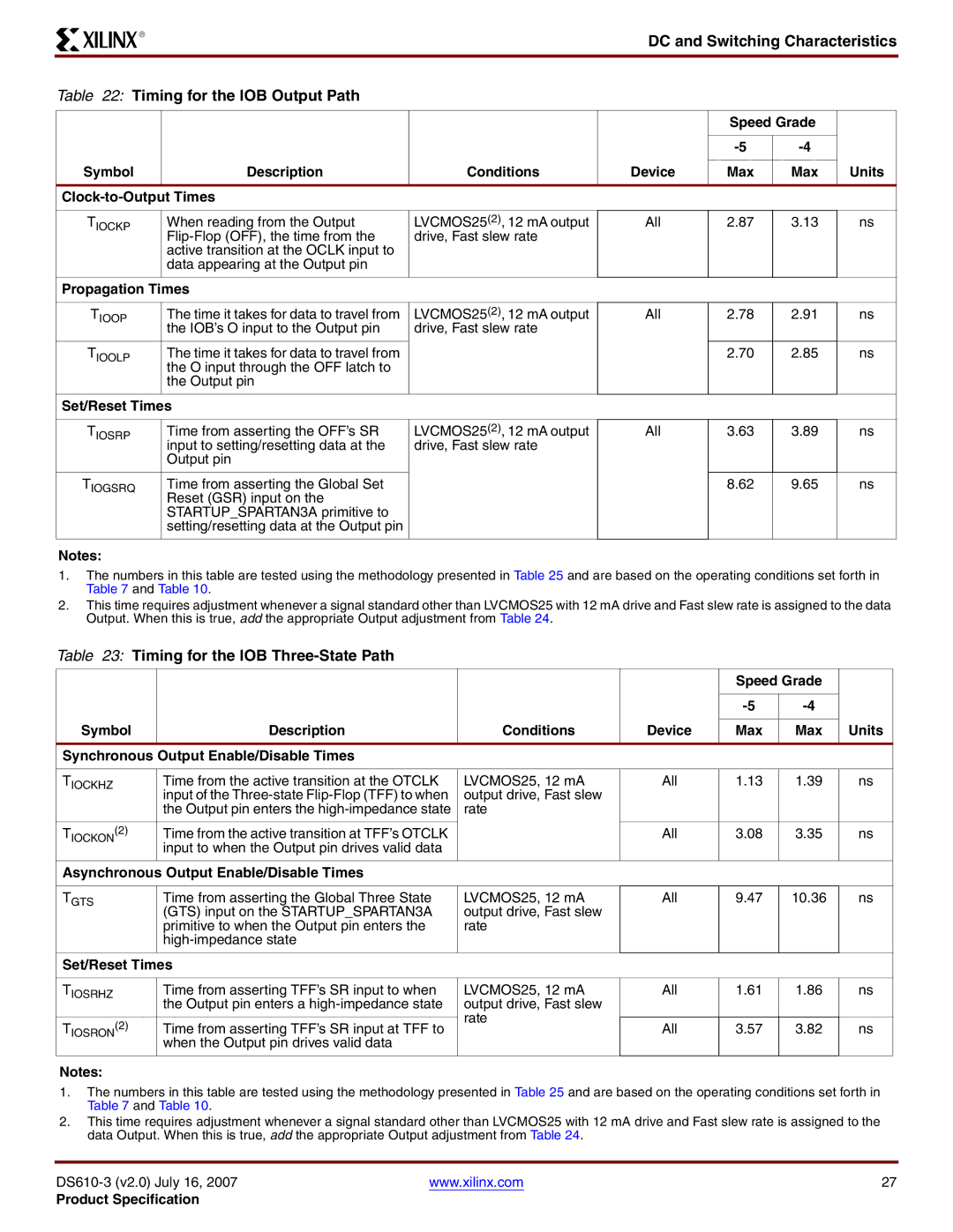
Table 22: Timing for the IOB Output Path
|
|
|
| Speed Grade |
| |
|
|
|
|
|
|
|
|
|
|
|
| ||
|
|
|
|
|
|
|
Symbol | Description | Conditions | Device | Max | Max | Units |
|
|
|
|
| ||
|
|
|
|
|
|
|
T | When reading from the Output | LVCMOS25(2), 12 mA output | All | 2.87 | 3.13 | ns |
IOCKP | drive, Fast slew rate |
|
|
|
| |
|
|
|
|
| ||
| active transition at the OCLK input to |
|
|
|
|
|
| data appearing at the Output pin |
|
|
|
|
|
|
|
|
|
|
|
|
Propagation Times |
|
|
|
|
| |
|
|
|
|
|
|
|
TIOOP | The time it takes for data to travel from | LVCMOS25(2), 12 mA output | All | 2.78 | 2.91 | ns |
| the IOB’s O input to the Output pin | drive, Fast slew rate |
|
|
|
|
|
|
|
|
|
|
|
TIOOLP | The time it takes for data to travel from |
|
| 2.70 | 2.85 | ns |
| the O input through the OFF latch to |
|
|
|
|
|
| the Output pin |
|
|
|
|
|
|
|
|
|
|
|
|
Set/Reset Times |
|
|
|
|
| |
|
|
|
|
|
|
|
T | Time from asserting the OFF’s SR | LVCMOS25(2), 12 mA output | All | 3.63 | 3.89 | ns |
IOSRP | input to setting/resetting data at the | drive, Fast slew rate |
|
|
|
|
|
|
|
|
| ||
| Output pin |
|
|
|
|
|
|
|
|
|
|
|
|
TIOGSRQ | Time from asserting the Global Set |
|
| 8.62 | 9.65 | ns |
| Reset (GSR) input on the |
|
|
|
|
|
| STARTUP_SPARTAN3A primitive to |
|
|
|
|
|
| setting/resetting data at the Output pin |
|
|
|
|
|
|
|
|
|
|
|
|
Notes:
1.The numbers in this table are tested using the methodology presented in Table 25 and are based on the operating conditions set forth in Table 7 and Table 10.
2.This time requires adjustment whenever a signal standard other than LVCMOS25 with 12 mA drive and Fast slew rate is assigned to the data Output. When this is true, add the appropriate Output adjustment from Table 24.
Table 23: Timing for the IOB Three-State Path
|
|
|
| Speed Grade |
| |
|
|
|
|
|
|
|
|
|
|
|
| ||
|
|
|
|
|
|
|
Symbol | Description | Conditions | Device | Max | Max | Units |
Synchronous Output Enable/Disable Times |
|
|
|
|
| |
|
|
|
|
|
|
|
TIOCKHZ | Time from the active transition at the OTCLK | LVCMOS25, 12 mA | All | 1.13 | 1.39 | ns |
| input of the | output drive, Fast slew |
|
|
|
|
| the Output pin enters the | rate |
|
|
|
|
|
|
|
|
|
|
|
TIOCKON(2) | Time from the active transition at TFF’s OTCLK |
| All | 3.08 | 3.35 | ns |
| input to when the Output pin drives valid data |
|
|
|
|
|
|
|
|
|
|
|
|
Asynchronous Output Enable/Disable Times |
|
|
|
|
| |
|
|
|
|
|
|
|
TGTS | Time from asserting the Global Three State | LVCMOS25, 12 mA | All | 9.47 | 10.36 | ns |
| (GTS) input on the STARTUP_SPARTAN3A | output drive, Fast slew |
|
|
|
|
| primitive to when the Output pin enters the | rate |
|
|
|
|
|
|
|
|
|
| |
|
|
|
|
|
|
|
Set/Reset Times |
|
|
|
|
| |
|
|
|
|
|
|
|
TIOSRHZ | Time from asserting TFF’s SR input to when | LVCMOS25, 12 mA | All | 1.61 | 1.86 | ns |
| the Output pin enters a | output drive, Fast slew |
|
|
|
|
|
| rate |
|
|
|
|
TIOSRON(2) | Time from asserting TFF’s SR input at TFF to |
| All | 3.57 | 3.82 | ns |
| when the Output pin drives valid data |
|
|
|
|
|
|
|
|
|
|
|
|
Notes:
1.The numbers in this table are tested using the methodology presented in Table 25 and are based on the operating conditions set forth in Table 7 and Table 10.
2.This time requires adjustment whenever a signal standard other than LVCMOS25 with 12 mA drive and Fast slew rate is assigned to the data Output. When this is true, add the appropriate Output adjustment from Table 24.
www.xilinx.com | 27 |
Product Specification
