R
Introduction and Ordering Information
IOBs
DCM
IOBs
|
|
|
|
|
| DCM |
| Slice |
|
|
|
|
|
|
|
|
|
|
|
|
|
| |
IOBs |
|
|
|
|
|
|
| DSP48A/RAM |
|
| IOBs |
|
| DCM |
| CLBs |
|
|
| ||||
|
|
|
|
|
|
|
|
| |||
|
|
|
|
|
|
|
|
| |||
|
|
|
|
|
|
|
| Block |
|
|
|
|
|
|
|
|
|
|
| ||||
|
|
|
|
|
|
|
|
|
|
|
|
|
|
|
|
|
|
|
|
|
|
|
|
IOBs
Notes:
CLB
Block RAM | DSP48A Slice |
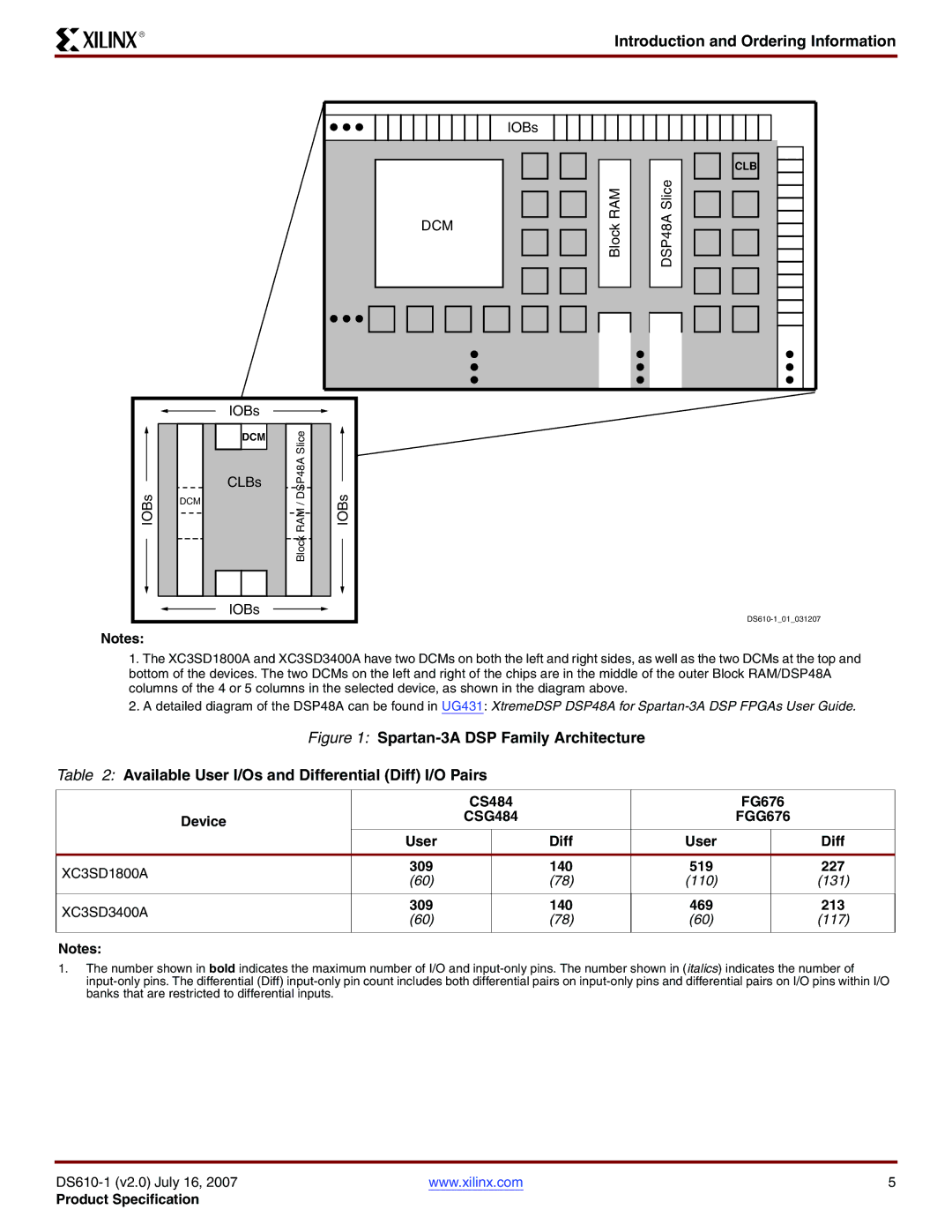
1. The XC3SD1800A and XC3SD3400A have two DCMs on both the left and right sides, as well as the two DCMs at the top and bottom of the devices. The two DCMs on the left and right of the chips are in the middle of the outer Block RAM/DSP48A columns of the 4 or 5 columns in the selected device, as shown in the diagram above.
2.A detailed diagram of the DSP48A can be found in UG431: XtremeDSP DSP48A for
Figure 1: Spartan-3A DSP Family Architecture
Table 2: Available User I/Os and Differential (Diff) I/O Pairs
|
|
| CS484 |
| FG676 | ||
| Device |
| CSG484 |
| FGG676 | ||
|
|
|
|
|
|
| |
|
| User |
| Diff | User |
| Diff |
XC3SD1800A |
| 309 |
| 140 | 519 |
| 227 |
| (60) |
| (78) | (110) |
| (131) | |
|
|
|
| ||||
|
|
|
|
|
|
|
|
XC3SD3400A |
| 309 |
| 140 | 469 |
| 213 |
| (60) |
| (78) | (60) |
| (117) | |
|
|
|
| ||||
|
|
|
|
|
|
|
|
Notes:
1.The number shown in bold indicates the maximum number of I/O and
www.xilinx.com | 5 |
Product Specification
