DC and Switching Characteristics
R
Block RAM Timing
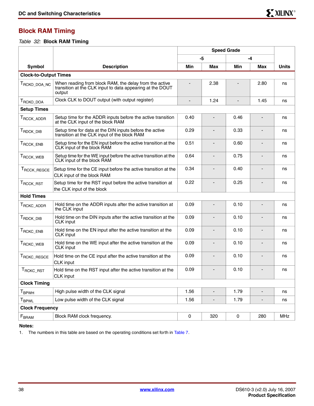
Table 32: Block RAM Timing
|
|
|
| Speed Grade |
|
|
| |
|
|
|
|
|
|
|
| |
|
|
|
|
| ||||
|
|
|
|
|
|
|
| |
Symbol | Description | Min |
| Max | Min |
| Max | Units |
|
|
|
|
|
|
| ||
|
|
|
|
|
|
|
|
|
TRCKO_DOA_NC | When reading from block RAM, the delay from the active | - |
| 2.38 | - |
| 2.80 | ns |
| transition at the CLK input to data appearing at the DOUT |
|
|
|
|
|
|
|
| output |
|
|
|
|
|
|
|
TRCKO_DOA | Clock CLK to DOUT output (with output register) | - |
| 1.24 | - |
| 1.45 | ns |
Setup Times |
|
|
|
|
|
|
|
|
|
|
|
|
|
|
|
|
|
TRCCK_ADDR | Setup time for the ADDR inputs before the active transition | 0.40 |
| - | 0.46 |
| - | ns |
| at the CLK input of the block RAM |
|
|
|
|
|
|
|
TRDCK_DIB | Setup time for data at the DIN inputs before the active | 0.29 |
| - | 0.33 |
| - | ns |
| transition at the CLK input of the block RAM |
|
|
|
|
|
|
|
TRCCK_ENB | Setup time for the EN input before the active transition at the | 0.51 |
| - | 0.60 |
| - | ns |
| CLK input of the block RAM |
|
|
|
|
|
|
|
TRCCK_WEB | Setup time for the WE input before the active transition at the | 0.64 |
| - | 0.75 |
| - | ns |
| CLK input of the block RAM |
|
|
|
|
|
|
|
TRCCK_REGCE | Setup time for the CE input before the active transition at the | 0.34 |
| - | 0.40 |
| - | ns |
| CLK input of the block RAM |
|
|
|
|
|
|
|
TRCCK_RST | Setup time for the RST input before the active transition at | 0.22 |
| - | 0.25 |
| - | ns |
| the CLK input of the block |
|
|
|
|
|
|
|
Hold Times |
|
|
|
|
|
|
|
|
|
|
|
|
|
|
|
|
|
TRCKC_ADDR | Hold time on the ADDR inputs after the active transition at | 0.09 |
| - | 0.10 |
| - | ns |
| the CLK input |
|
|
|
|
|
|
|
TRDCK_DIB | Hold time on the DIN inputs after the active transition at the | 0.09 |
| - | 0.10 |
| - | ns |
| CLK input |
|
|
|
|
|
|
|
TRCKC_ENB | Hold time on the EN input after the active transition at the | 0.09 |
| - | 0.10 |
| - | ns |
| CLK input |
|
|
|
|
|
|
|
TRCKC_WEB | Hold time on the WE input after the active transition at the | 0.09 |
| - | 0.10 |
| - | ns |
| CLK input |
|
|
|
|
|
|
|
TRCKC_REGCE | Hold time on the CE input after the active transition at the | 0.09 |
| - | 0.10 |
| - | ns |
| CLK input |
|
|
|
|
|
|
|
TRCKC_RST | Hold time on the RST input after the active transition at the | 0.09 |
| - | 0.10 |
| - | ns |
| CLK input |
|
|
|
|
|
|
|
Clock Timing |
|
|
|
|
|
|
|
|
|
|
|
|
|
|
|
|
|
TBPWH | High pulse width of the CLK signal | 1.56 |
| - | 1.79 |
| - | ns |
TBPWL | Low pulse width of the CLK signal | 1.56 |
| - | 1.79 |
| - | ns |
Clock Frequency |
|
|
|
|
|
|
| |
|
|
|
|
|
|
|
|
|
FBRAM | Block RAM clock frequency. | 0 |
| 320 | 0 |
| 280 | MHz |
Notes:
1.The numbers in this table are based on the operating conditions set forth in Table 7.
38 | www.xilinx.com | |
|
| Product Specification |
