DL-V3
Proprietary Notice
Table of Contents
Oemv Family Receiver Performance DL-V3 Specifications
Extcontrol Disable Automatic Powerup Group
Control COM Power for a Group 103
Edit Group Dgps ID Configuration 105
Table of Contents
114
115
116
Bluetooth Configuration 195
Figures
198
197
199
Tables
Tables
126
134
136
Software License
Restrictions You may not
Software License
Terms and Conditions
Standard Terms and Conditions of Sales
Terms and Conditions
Warranty
FCC Notices
What is the hazard?
Lightning Protection Notice
Hazard Impact
Actions to Mitigate Lightning Hazards
DL-V3 Regulatory Testing
Electromagnetic Compatibility EMC and Safety
Description
Weee Notice
RoHS Notice
Customer Service
Oemv Firmware Upgrades
Foreword
Congratulations
Scope
Prerequisites
Conventions
Foreword
Chapter Introduction
Model Name Firmware Feature
DL-V3 Controller Models
GPS Positioning Modes of Operation
Chapter Introduction
Modes of Operation a DL-V3 Model RT20 L1/L2
Chapter Installation and Setup
DL-V3 Setup
Chapter Installation and Setup
Antenna Port
Installation and Setup Chapter
Ethernet Port
DB-9 Setup
Bluetooth Setup
Installing the PC Utilities
Selecting a Gnss Antenna
Power Supply Requirements
Choosing a Coaxial Cable
NovAtel Gnss Antenna Models
Models Frequencies Supported
Connecting the Antenna to the Receiver
Applying Power to the Receiver
Enclosure Power Requirements
Mounting Bracket
Connecting Data Communications Equipment
DL-V3 Power Down and the Power Button
Default Serial Port Configurations
Receiver
Strobes
DL-V3 COM3 Configuration
Universal Serial Bus USB
Power
Status Indicators
Status Communication Ports excluding COM3
Positioning Mode
Satellite Tracking
Satellite Tracking LEDs
Flash Card Memory
Positioning Mode LEDs
Position Mode Position Mode Detail a
External Oscillator
Occupation Time
Occupation Time LEDs
Baseline Length LED Color
Antenna LNA Power
DL-V3 Removable Compact Flash Memory Card
Access Door
Data Logging
Using CDU to Format the CF Card
Card Choice
Using HyperTerminal to Format the CF Card
Installation and Setup Chapter
Serial Port Default Settings
Chapter Operation
Communicating Using a Remote Terminal
Communicating Using a Personal Computer
Communicating with the Receiver Using CDU
Starting the Receiver
Chapter Operation
Transmitting and Receiving Corrections
Rover Base
Base Station Configuration
Log port message trigger period
Rover Station Configuration
Configuration Notes
Using the DL-V3
Log Data from a Site to a File
Edit the Site
Select the Group
Start the Data Logging
Enabling Sbas Positioning
Stop the Data Logging
Pass-Through Logging
Sync Option
Chapter DL Explorer
Starting DL Explorer
Receiver Groups
Exiting DL Explorer
DL Explorer Chapter
Chapter DL Explorer
Logs Tab
Log Triggers
Trigger Description
Preset Powerup Group
Position Tab
Position Tab
Site Tab
Site Tab
Interfaces Tab
Interfaces Tab
Ports Tab
Ports Tab
Communication Parameters
COM Parameters
Upload Group from the PC/Laptop to the Receiver
Group Management
Starting Groups
Transfer a File from the DL-V3 to the PC/Laptop
Log Transfer Dialog
File Details
Flight Recorder
Flight Recorder OFF
CF Card Status
CF Card Status
Appendix a
Oemv Family Receiver Performance
DL-V3 Specifications
Color
Baseline
LEDs Color
Length km Color
Dimensions
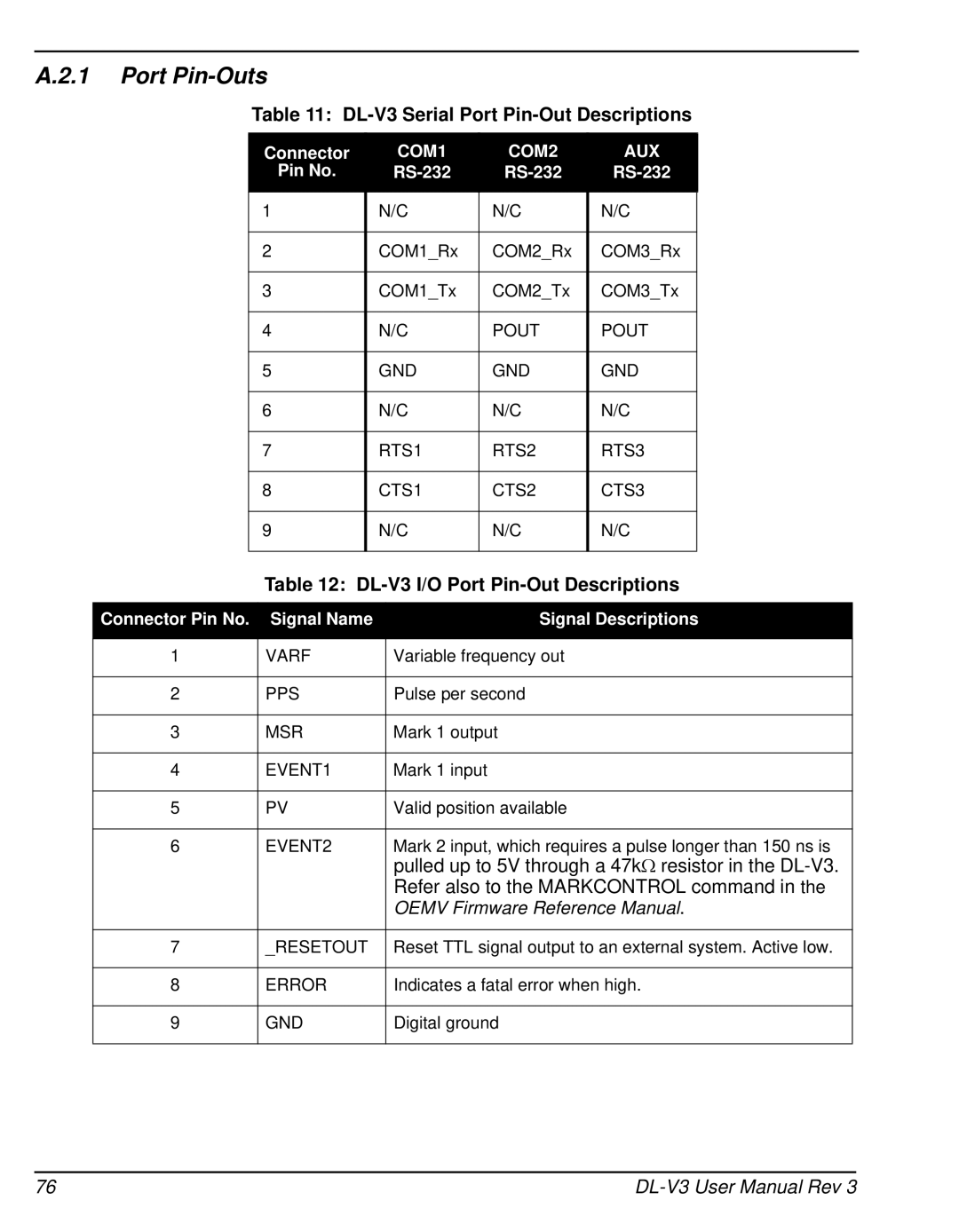
DL-V3 I/O Port Pin-Out Descriptions
DL-V3 Serial Port Pin-Out Descriptions
Oemv Firmware Reference Manual
2.1 12V Power Adapter Cable NovAtel part number
DL-V3 Power Cable
Null-modem Cable NovAtel part number
Reference Description
Straight Through Serial Cable NovAtel part number
DL-V3 Straight Through Serial Cable
Wiring Table
2.4 I/O Strobe Port Cable NovAtel part number
DL-V3 Commands in Alphabetical Order
Message ID Ascii Command Description
DL-V3 Commands in Order of their Message IDs
Message ID Ascii Command Description
Syntax Conventions
Appcontrol COM3 Bluetooth/Ethernet Switch
Dhcp OFF
Application Functions
Application Parameters
Binary
BinaryASCII
Comvout Control COM Peripheral Power
COM Serial Port Identifiers
Default
COM Voltage Out Action
Dump Mode
Currentfile Default Configuration
Parameter Power-On Freset Stored in NVM
Currentfile Specify File for FILEHDR/FILETRANSER Logs
Currentgroup Default Configuration
Currentgroup Specify File for Groupdef Log
DEL Delete Files from CF Card
Delete Target
Disk Format the CF Card
CF Card Operation
Extcontrol Disable Automatic Powerup Group
Freset Clear Selected Data from NVM and Reset
Freset Target
Group Create and Manipulate Groups
Group Default Configuration
Action
Groupantheight Default Configuration
Groupantheight Edit Group Antenna Height
Groupantsn Default Configuration
Groupantsn Edit Group Antenna Serial Number
Groupanttype Default Configuration
Groupanttype Edit Group Antenna Type
Groupcom Associate Port Configurations with a Group
Parameter Update
101
Handshaking
Parity
102
Groupcomvout Control COM Power for a Group
Example
104
Groupdgpstxid Edit Group Dgps ID Configuration
Dgps Type, see on Page 165 and Table
Field Power-On Freset Stored in NVM
Groupdgpstxid Default Configuration
106
Groupecutoff Default Configuration
Groupecutoff Edit Group Elevation Cut-Off Angle
Groupfixpos Configure Group to Fix Receiver Position
Groupfixpos Default Configuration
Groupinterfacemode Edit Group Interface Mode
Parameter Power-On Freseta Stored in NVM
Groupinterfacemode Default Configuration
110
Grouplog Edit Group Logging Specifications
Grouplog Default Configuration
112
Group Mode
Groupmode Configure Group Survey Type
Groupmode Default Configuration
Groupposave Configure Group Position Averaging
Groupsave Default Configuration
Groupsatlimit Default Configuration
Groupsatlimit Limit Number of Satellites for Group
Groupsitename Default Configuration
Groupsitename Edit Group Site Name
Groupsitenumber Default Configuration
Groupsitenumber Edit Group Site Number
Groupuse Execute a Set of Commands
Log hdrdst versionb command is issued
Group Action
119
LOG Request Logs from the Receiver
Factory Default
121
122
Description Field Name Value Type
Detailed Serial Port Identifiers
123
124
XCOM3
Logfile Open or Close File on CF Card
Logfile Default Configuration
Log File Action
Methumid Default Configuration
Methumid Specify Air Humidity
Metpress Default Configuration
Metpress Specify Air Pressure
Mettemp Specify Air Temperature
Mettemp Default Configuration
Project Add or Clear a Project
Project Default Configuration
Project Action
Rename Rename a File on the CF Card
Reset Perform a Hardware Reset
Satlimit Set Minimum Satellites in Position Solution
Satlimit Default Configuration
File Port Channel
Site Control Site Occupations
Site Mode
Site Default Configuration
Siteupdatenumber Set Occupied Site Number
Siteupdatenumber Default Configuration
Siteupdatename Set Occupied Site Name
Siteupdatename Default Configuration
Siteupdateantheight Set Occupied Site Height
Siteupdateantheight Default Configuration
Siteupdateanttype Set Occupied Site Antenna
Siteupdateanttype Default Configuration
Siteupdateattribute Set Occupied Site Attributes
Siteupdateattribute Default Configuration
Softpower Simulate a Power-Button Off
Softpower
Write Create User Data Logs
Writefile Create/Append Files on CF Card
Writefilehex Create/Append Data to CF Card
Writehex Create User Data Logs
DL-V3 Logs in Alphabetical Order
Message ID Ascii Log Description
DL-V3 Logs in Order of their Message IDs
Message Ascii Log Description
PDC Log Header
Type Size Description Range Offset
Serial Port Identifiers
Port Identifier Description
Binary Value Ascii Mode Name Description
Serial Port Interface Modes
152
Generic
Currentset CURRENTFILE/CURRENTGROUP Configuration
Field Data Description Bytes Format Units Offset
Dirent CF Card File List
155
Extlevels Extended Hardware Levels
Filechannel Log File Channel Configuration
Filehdr
Logfile Header
File Status
File Status Bit Description Bit=0 Bit=1
Filetransfer Log File Contents
Groupcomconfig COM Port Configuration Information
Groupcomconfig Status Word
Status Bit Description Bit=0 Bit=1
Groupdef Log Group Configuration
164
COM1/COM2 Interface Modes
Dgps Type
Dgps Type Description Binary
Group Status1 Word
Group Status Bit Description Bit=0 Bit=1
Group Status2 Word
Meteorological Log Status
Metdef Meteorological Parameters
Met Status Bit Description Bit=0 Bit=1
Projectdef
Pwrstatus Power and Status Settings Summary
DL-V3 Voltage Parameter Logs
Port Power Status
Power Status Bits Description Bit =
Auxiliary 2 Status Word
Rxstatus DL-V3 Status
AUX2 Bit Description Bit=0 Bit=1 Trigger
Auxiliary 3 Status Word
AUX3 Bit Description Bit=0 Bit=1 Trigger
174
Rxstatusevent DL-V3 Status Event Notification
Site Status
Site Configuration
SiteStatus Bit Bit Name Description Bit=0 Bit=1
Version HW & SW Versions and Serial Numbers
Write User-Generated Information
Writehex User-Generated Information
Component Type
Appendix D
Physical Set-Up
Configuration Overview
179
Enable Ethernet on the DL-V3 Receiver
180
181
182
183
184
Network Settings Configuration
185
Lantronix COM Redirector Manager
186
Add the DL-V3 Ethernet Device’s IP Address and Port
Configure Virtual Serial Port
187
Redirector Configuration Completion
Alternative Serial Configuration
188
HyperTerminal Default Parameters
Switch to Ethernet Device
Reset Ethernet
Establish Serial Command Mode in Ethernet
Establish a Communications Tunnel
190
Command Mode Example
191
Network Configuration in Command Mode
192
193
194
Set Up a PC/Laptop with a Bluetooth Adaptor
Enable Bluetooth on the DL-V3 Receiver
195
Locate a Bluetooth-Enabled DL-V3 in Range
196
Communicate with the DL-V3 Using Bluetooth
Bluetooth PIN Code Request
Stop Communicating with the DL-V3 Using Bluetooth
Bluetooth Connected Green
COM3 Disconnect?
Manufacturer’s Part Number
Accessories
200
Index
201
Index
202
CF card, 39, 41, 92 collect, 40, 51, 53
203
Bluetooth, 27
204
LED
205
Base, 47, 49
206
RTK, 24
207
OM-20000119 Rev 2009/07/22