Chapter 3: Hardware Description
R
also be supplied from a bench supply using the two banana jacks: J25 (RED) for +5V and J24 (BLACK) for GND.
The
The memory and FPGAs use separate power supplies for SSTL18, HSTL, and SSTL2, respectively. Thus the power being consumed can be easily measured for each using the power measurement header provided on the ML561.
Voltage Regulators
The +5V voltage source is supplied as input to nine
An additional three bulk voltage regulators (Fairchild FN6555) are used to generate termination (VTT) and reference (VREF) voltages each for the SSTL2, SSTL18, and HSTL power levels. By design, these voltage levels are half of the input reference voltage being supplied by the memory power supplies.
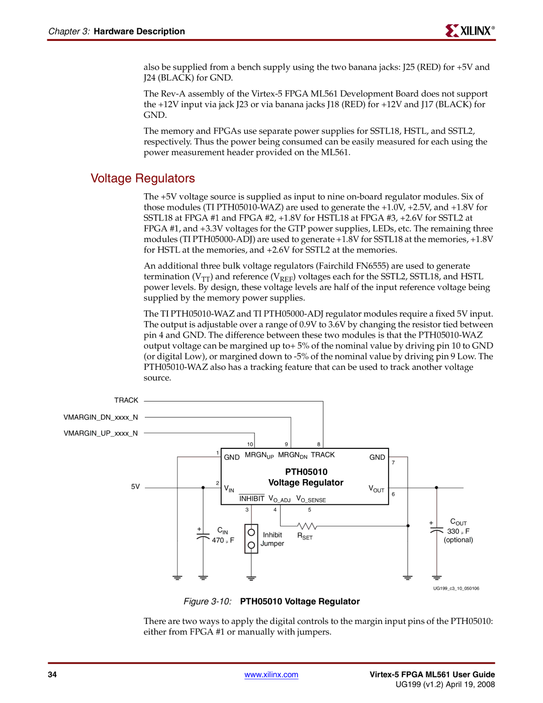
The TI
TRACK
VMARGIN_DN_xxxx_N
VMARGIN_UP_xxxx_N
5V
|
|
|
|
|
|
|
|
|
|
|
|
|
|
|
|
|
|
|
|
|
|
|
|
| 10 | 9 | 8 |
|
|
|
| 1 |
| GND | MRGNUP MRGNDN TRACK | GND | |||
|
|
|
| ||||||
|
|
|
|
|
|
|
|
|
|
|
|
|
|
|
|
|
|
|
|
|
|
|
|
|
|
| PTH05010 |
|
|
|
|
|
|
|
|
| 2 |
|
|
|
|
|
|
|
|
|
|
|
| Voltage Regulator | |||||
|
|
|
|
|
|
|
|
|
|
|
|
|
|
| VIN |
|
|
|
|
|
| VOUT | |||||
|
|
|
|
|
|
|
|
|
|
|
|
|
|
|
|
|
|
|
|
| |||||||
|
|
|
|
|
|
|
|
|
|
|
|
|
|
|
| INHIBIT | VO_ADJ VO_SENSE | ||||||||||
|
|
|
|
|
|
|
|
| 3 |
| 4 | 5 | |||||||||||||||
|
|
|
|
| + |
|
|
|
|
|
|
|
|
|
|
|
|
|
| ||||||||
|
|
|
|
|
|
|
|
|
| CIN |
|
|
|
|
| Inhibit | RSET | ||||||||||
|
|
|
|
|
|
|
|
|
|
|
|
|
| ||||||||||||||
|
|
|
|
|
|
|
|
|
|
|
|
| 470 μF |
|
|
|
|
|
|
|
| ||||||
|
|
|
|
|
|
|
|
|
|
|
|
|
|
|
|
| |||||||||||
|
|
|
|
|
|
|
|
|
|
|
|
|
|
|
|
|
| Jumper |
| ||||||||
|
|
|
|
|
|
|
|
|
|
|
|
|
|
|
|
|
|
|
|
|
|
|
|
|
| ||
|
|
|
|
|
|
|
|
|
|
|
|
|
|
|
|
|
|
|
|
|
|
|
|
|
|
|
|
|
|
|
|
|
|
|
|
|
|
|
|
|
|
|
|
|
|
|
|
|
|
|
|
|
|
|
|
|
|
|
|
|
|
|
|
|
|
|
|
|
|
|
|
|
|
|
|
|
|
|
|
|
|
|
|
7
6
+
COUT
330μF
(optional)
UG199_c3_10_050106
Figure 3-10: PTH05010 Voltage Regulator
There are two ways to apply the digital controls to the margin input pins of the PTH05010: either from FPGA #1 or manually with jumpers.
34 | www.xilinx.com |
|
|
| UG199 (v1.2) April 19, 2008 |
