UG199 v1.2 April 19
Virtex-5 Fpga ML561 Memory Interfaces Development Board
Date Version Revision
Revision History
Table of Contents
Electrical Requirements
Appendix B Bill of Materials Appendix C LCD Interface
Virtex-5 Fpga ML561 User Guide
About This Guide
Guide Contents
Additional Documentation
Preface About This Guide
Additional Support Resources
Terminology
Conventions
Typographical
Online Document
Virtex-5 Fpga ML561 User Guide
About the Virtex-5 Fpga ML561 Memory Interfaces Tool Kit
Introduction
Introduction
Virtex-5 Fpga ML561 Memory Interfaces Development Board
2Virtex-5 Fpga ML561 Development Board
Virtex-5 Fpga ML561 Memory Interfaces Development Board
Introduction
Getting Started
Initial Board Check Before Applying Power
Documentation and Reference Design CD
Getting Started
Applying Power to the Board
Hardware Overview
Hardware Description
Hardware Description
1ML561 XC5VLX50T-FFG1136 Board Placement Diagram
DDR400 Sdram Components
Memories
Hardware Overview
Rldram II Devices
DDR2 Sdram Components
DDR400 and DDR2 Component Memories
Memory Details
Memory Details
DDR2ODT10, DDR2RAS,CAS,WEN
DDR1RAS,CAS,WEN, DDR1CKE
DDR2 Sdram Dimm
Dimm
DDR2DIMMRAS,CAS,WE,RESETN
DDR2DIMM15CNTLPAR
DDR2DIMM15CNTLPARERR
Qdrii and Rldram II Memories
QDR2R,W,DLLOFFN
RS-232
External Interfaces
Clocks
SMA Clock
MHz Lvpecl Clock
MHz Clock
User I/Os
DIP Switch
MHz System ACE Controller Oscillator
GTP Clocks
Seven-Segment Displays
Seven-Segment Display Signal Mapping
Light Emitting Diodes LEDs
Pushbuttons
Power Measurement Header
Power On or Off Slide Switch
Soft Touch Probe Points
Liquid Crystal Display Connector
Power Distribution
Power Regulation
Power Regulation
10PTH05010 Voltage Regulator
Voltage Regulators
Output Voltage
16Manual Voltage Margining
Board Design Considerations
11ML561 Revision a PCB Stack-Up
Board Design Considerations
TOP
19ML561 Revision a PCB Controlled Impedance
Electrical Requirements
Power Consumption
Power Consumed DDR400 Component Interface
Total Available Power
Total Power Consumed
Current
Power Modules Capacity
Electrical Requirements
2Power Planes Voltage Regulator Module VRM Part
Stack-Up
3ML561 Power Plane Capacities
Power Consumption
Current Power Excess Device Description Quantity
Power Consumed by Power Plane
Electrical Requirements 3ML561 Power Plane Capacities
Current Power Excess Device Description
Power Consumption 3ML561 Power Plane Capacities
Total Power Consumed 53.2
4ML561 Fpga Power Estimate Summary
Fpga Internal Power Budget
Fpga #21
Termination and Transmission Line Summaries
Signal Integrity Recommendations
2DDR2 Sdram Dimm Terminations Signal Fpga Driver
HSTLI18
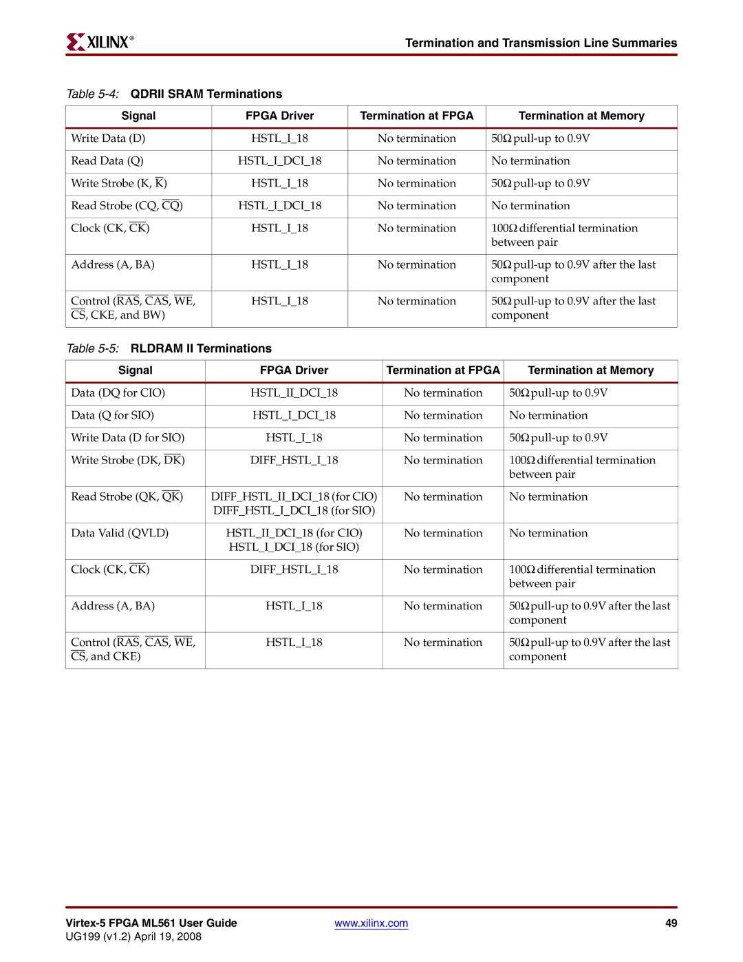
5RLDRAM II Terminations Signal
HSTLIDCI18
HSTLIIDCI18
Signal Integrity Recommendations
Configuration Modes
Configuration
Jtag Chain
Configuration 1Configuration Modes
Jtag Port
Parallel IV Cable Port
System ACE Interface
Configuration
Introduction
ML561 Hardware-Simulation Correlation
ML561 Hardware-Simulation Correlation
Test Setup
1Single Trapezoid Eye Mask Definition
Test Setup
2Two Triangular Eye Mask Definitions for VIH and VIL
Signal Integrity Correlation Results
DDR2 Component Write Operation
Signal Integrity Correlation Results
2DDR2 Component Write Operation Correlation Results
Measurement
3DIP12 Settings Description
Voltage mV
Voltage mV
Time ns
UG199c711071007
Fpga SSTL18IIDCII
DDR2 Component Read Operation
5DDR2 Component Read Operation Correlation Results
Time ns
UG199c715071107
UG199c717071007
UG199c719071007
DDR2 DIMM, 75 Ω ODT
DDR2 Dimm Write Operation
Noise Margin Overshoot / Undershoot Measurement
8DIP12 Settings Description
UG199c722071107
UG199c724071107
UG199c726071007
UG199c729071007
10DDR2 Dimm Read Operation Correlation Results DVW %
DDR2 Dimm Read Operation
UG199c731071107
1800.0 1600.0 1400.0 1200.0 1000.0
UG199c735071007
UG199c737071007
Fpga HSTLI18
Qdrii Write Operation
12 Qdrii Write Operation Correlation Results
800.0 600.0 400.0 200.0 000 Probe 3C7.1 at pin 1200.0 1600.0
UG199c742071107
UG199c744070907
3100.0 2600.0 2100.0 1600.0 1100.0
Fpga HSTLIDCI18
Qdrii Read Operation
14QDRII Read Operation Correlation Results
UG199c749071107
1900.0 1700.0 1500.0 1300.0 1100.0
UG199c753070907
UG199c755070907
Summary and Recommendations
Summary and Recommendations
Noise Margin Overshoot Operation
16Summary of Worst-Case SI Characteristics
How to Generate a User-Specific Fpga Ibis Model
How to Generate a User-Specific Fpga Ibis Model
ML561 Hardware-Simulation Correlation
Fpga #1 Pinout
Fpga Pinouts
Table A-1FPGA #1 Pinout Signal Name
Fpga #1 Clock and Reset Signals
FPGA3TOFPGA1MIITXCLK
FPGA2TOFPGA1MIITXCLK
FPGA2TOFPGA1MIITXDATA0
FPGA3TOFPGA1MIITXDATA0
Fpga #1 Pinout Table A-1FPGA #1 Pinout Signal Name
Fpga #2 Pinout
DDR2DIMMDQBY0B4
DDR2DIMM3CK2P
DDR2DIMM3CKE0
DDR2DIMMDQBY0B5
DDR2DIMMDQBY7B7
DDR2DIMMDQBY4B4
DDR2DIMMDQBY4B5
DDR2DIMMDQCB07B0
DDR2DIMMDQBY11B5 DDR2DIMM5CS1N
DDR2DIMM5CS0N
DDR2DIMMDQBY11B6
DDR2DIMM5ODT0 AA9 DDR2DIMMDQBY11B7
Table A-2FPGA #2 Pinout Signal Name
Fpga #2 Clock and Reset Signals
Fpga #2 Pinout Table A-2FPGA #2 Pinout Signal Name
FPGA2SOFTTOUCHBY1B7
FPGA2DIP0
FPGA2DIP1
FPGA2SPYHOLEBK15
FPGA2TXN1BK120 FPGA2USBDSRN
FPGA2TXN0BK120 FPGA2USBCTSN
FPGA2TXP0BK120 FPGA2USBDTRN
FPGA2TXP1BK120 FPGA2USBRSTN
Fpga #3 Pinout
Table A-3FPGA #3 Pinout Signal Name Qdrii Memory Interface
QDR2DBY4B1
QDR2DBY0B5
QDR2DBY0B6
QDR2DBY4B2
QDR2QBY3B2
QDR2DBY7B6
QDR2DBY7B7
QDR2QBY3B3
QDR2QBY7B4
QDR2QBY6B7
QDR2QBY6B8
QDR2QBY7B5
RLD2DBY0B7 RLD2DQBY0B1
RLD2DBY0B5 RLD2DMBY23N RLD2DBY0B6 RLD2DQBY0B0
RLD2DBY0B8 RLD2DQBY0B2 RLD2DBY1B0
RLD2DQBY0B3
RLD2DQBY3B4 RLD2DQBY3B7 RLD2DQBY3B5 RLD2DQBY3B8 RLD2DQBY3B6
FPGA3RESETNIN
CLKTOFPGA3MGTN EXTCLKTOFPGA3N
CLKTOFPGA3MGTP EXTCLKTOFPGA3P
Table A-3FPGA #3 Pinout Signal Name
Table B-1Bill of Materials
Bill of Materials
4A LDO
Appendix B Bill of Materials Table B-1Bill of Materials
Virtex-5 Fpga ML561 User Guide 117
Appendix B Bill of Materials
General
LCD Interface
Display Hardware Design
Table C-1Display Controller Specifications Parameter
Hardware Schematic Diagram
Appendix C LCD Interface
Peripheral Device KS0713
Hardware Schematic Diagram
64128EFCBC-XLP Block Diagram
Table C-2 LCD Panel
Controller Operation
124
Controller LCD Panel Connections
Figure C-5Power Supply Circuits
Controller Power Supply Circuits
Figure C-6LCD Controller Initialization Flow
Operation Example of the 64128EFCBC-3LP
OFF
Table C-5 Reference Voltage Parameters
Table C-4Resistor Value Settings
Reference Voltage Parameter α
Table C-6Display Instructions
Instruction Set
Set page address
Hardware Schematic Diagram Table C-6Display Instructions
EON
Appendix C LCD Interface Table C-6Display Instructions
ERD
Read/Write Characteristics 6800 Mode
Design Examples
LCD Panel Used in Full Graphics Mode
Display Command Byte
LCD Panel Used in Character Mode
Display Data Byte
Figure C-10Block RAM Organization
Figure C-11LCD Character Generator Controller
C D E F G H
Array Connector Numbering
140