Chapter 1: Introduction
R
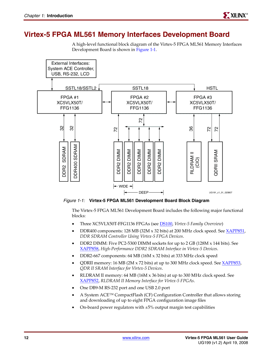
Virtex-5 FPGA ML561 Memory Interfaces Development Board
A
External Interfaces:
System ACE Controller,
USB,
SSTL18/SSTL2 ![]()
FPGA #1
XC5VLX50T/
FFG1136
32 |
| 32 |
| |
|
|
|
|
|
|
|
|
|
|
DDR2 SDRAM |
| DDR400 SDRAM | ||
|
|
|
|
|
SSTL18
FPGA #2
XC5VLX50T/
FFG1136
|
|
|
|
|
|
|
|
|
| 72 |
|
|
|
|
|
|
|
| |||
72 |
|
|
|
|
|
|
|
|
|
|
|
|
|
|
|
|
|
|
|
| |
|
|
|
|
|
|
|
|
|
|
|
|
|
|
|
|
|
|
|
| ||
|
|
|
|
|
|
|
|
|
|
|
|
|
|
|
|
|
|
|
| ||
|
|
|
|
|
|
|
|
|
|
|
|
|
|
|
|
|
|
| |||
|
|
|
|
|
|
|
|
|
|
|
|
|
|
|
|
|
|
|
|
|
|
|
|
|
|
|
|
|
|
|
|
|
|
|
|
|
|
|
|
|
|
|
|
| DDR2 DIMM |
|
|
| DDR2 DIMM |
| DDR2 DIMM |
| DDR2 DIMM |
| DDR2 DIMM | ||||||||||
|
|
|
|
|
|
|
|
|
|
|
|
|
|
|
|
|
|
|
|
|
|
|
|
|
|
|
|
|
|
|
|
|
|
|
|
|
|
|
|
|
| ||
|
|
| WIDE |
|
|
|
|
|
|
|
|
|
|
|
|
|
| ||||
|
|
|
|
|
|
|
|
|
|
|
|
|
|
|
| ||||||
|
|
|
|
|
|
|
|
|
|
|
|
|
|
|
|
|
|
| |||
|
|
|
|
|
|
|
|
|
|
|
| DEEP |
|
|
|
|
|
| |||
|
|
|
|
|
|
|
|
|
|
|
|
|
|
|
|
|
| ||||
|
|
|
|
|
|
|
|
|
|
|
|
|
|
|
|
|
|
|
|
|
|
HSTL
FPGA #3
XC5VLX50T/
FFG1136
| 36 |
| 72 | 72 |
|
| |
|
|
|
| ||||
|
|
|
|
|
|
|
|
|
|
|
|
|
|
|
|
| RLDRAM II (CIO) |
|
| QDRII SRAM |
| ||
|
|
|
|
|
|
|
|
UG191_c1_01_020807
Figure 1-1: Virtex-5 FPGA ML561 Development Board Block Diagram
The
•Three
•DDR400 components: 128 MB (32M x 32 bits) at 200 MHz clock speed. See XAPP851, DDR SDRAM Controller Using
•DDR2 DIMM: Five
•
•QDRII memory: 16 MB (2M x 72 bits) at up to 300 MHz clock speed. See XAPP853, QDR II SRAM Interface for
•RLDRAM II memory: 64 MB (16M x 36 bits) at up to 300 MHz clock speed. See XAPP852, RLDRAM II Memory Interface for
•One
•A System ACE™ CompactFlash (CF) Configuration Controller that allows storing and downloading of up to eight FPGA configuration image files
•
12 | www.xilinx.com |
|
|
| UG199 (v1.2) April 19, 2008 |