Chapter 7: ML561 Hardware-Simulation Correlation
R
VOH(dc)
VIH(dc)
VIL(dc)
VDDQ
VIH(ac)
VREF
VIL(ac)
VOH(ac)
VOL(dc)
VOL(ac)
VSS
UG199_c7_02_062707
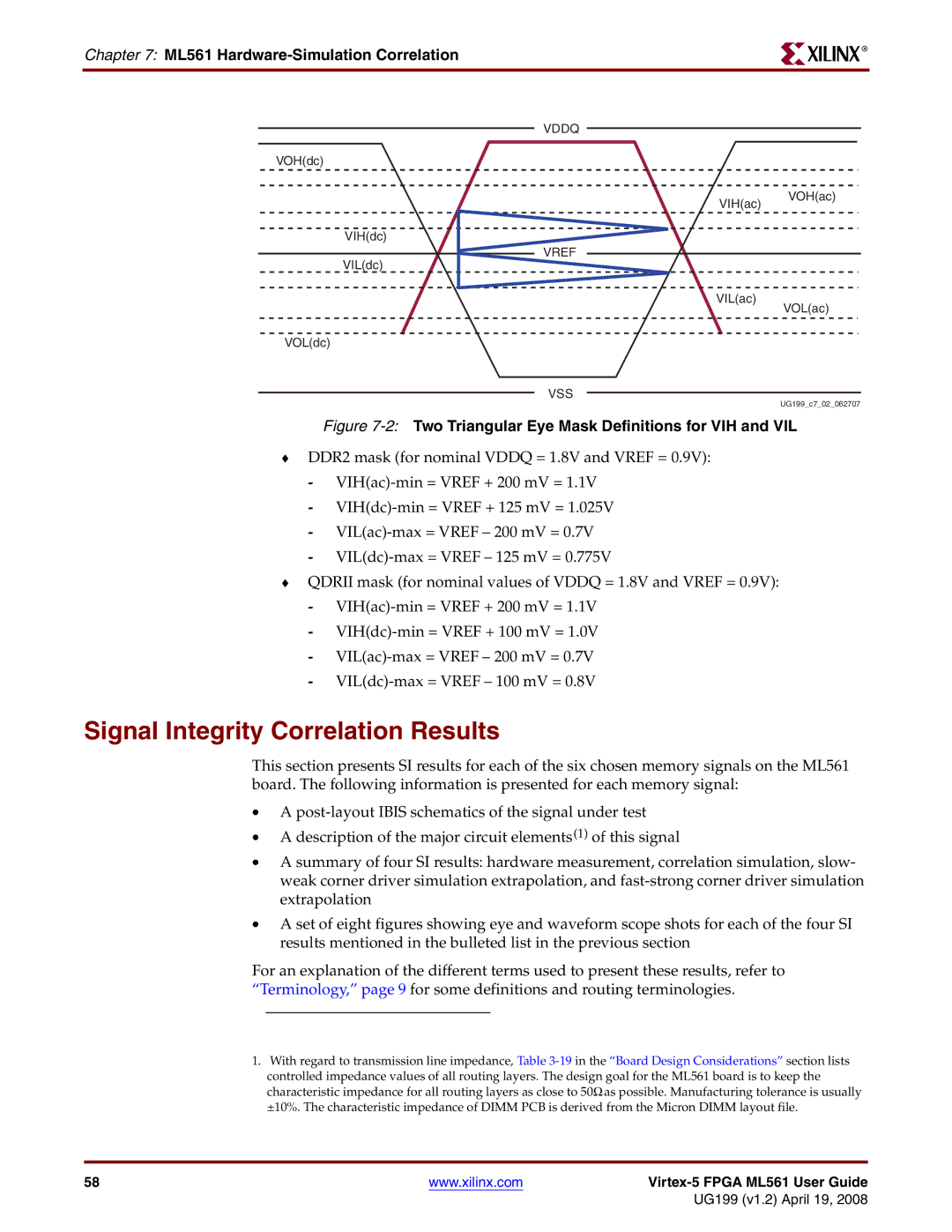
Figure 7-2: Two Triangular Eye Mask Definitions for VIH and VIL
♦DDR2 mask (for nominal VDDQ = 1.8V and VREF = 0.9V):
-
-
-
-
♦QDRII mask (for nominal values of VDDQ = 1.8V and VREF = 0.9V):
-
-
-
-
Signal Integrity Correlation Results
This section presents SI results for each of the six chosen memory signals on the ML561 board. The following information is presented for each memory signal:
•A
•A description of the major circuit elements(1) of this signal
•A summary of four SI results: hardware measurement, correlation simulation, slow- weak corner driver simulation extrapolation, and
•A set of eight figures showing eye and waveform scope shots for each of the four SI results mentioned in the bulleted list in the previous section
For an explanation of the different terms used to present these results, refer to “Terminology,” page 9 for some definitions and routing terminologies.
1.With regard to transmission line impedance, Table
controlled impedance values of all routing layers. The design goal for the ML561 board is to keep the characteristic impedance for all routing layers as close to 50Ω as possible. Manufacturing tolerance is usually ±10%. The characteristic impedance of DIMM PCB is derived from the Micron DIMM layout file.
58 | www.xilinx.com |
|
|
| UG199 (v1.2) April 19, 2008 |
