Chapter 4: Electrical Requirements
R
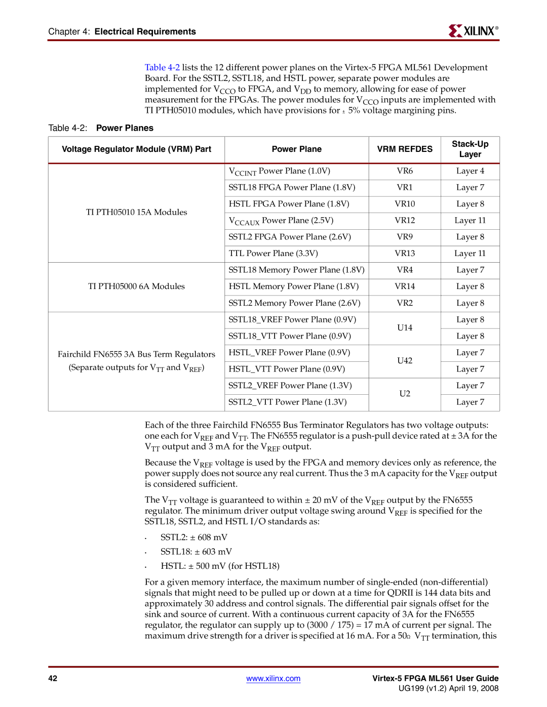
Table
Table 4-2: Power Planes
Voltage Regulator Module (VRM) Part | Power Plane | VRM REFDES |
| |
Layer | ||||
|
|
| ||
|
|
|
| |
| VCCINT Power Plane (1.0V) | VR6 | Layer 4 | |
| SSTL18 FPGA Power Plane (1.8V) | VR1 | Layer 7 | |
|
|
|
| |
TI PTH05010 15A Modules | HSTL FPGA Power Plane (1.8V) | VR10 | Layer 8 | |
|
|
| ||
VCCAUX Power Plane (2.5V) | VR12 | Layer 11 | ||
| ||||
| SSTL2 FPGA Power Plane (2.6V) | VR9 | Layer 8 | |
|
|
|
| |
| TTL Power Plane (3.3V) | VR13 | Layer 11 | |
|
|
|
| |
| SSTL18 Memory Power Plane (1.8V) | VR4 | Layer 7 | |
|
|
|
| |
TI PTH05000 6A Modules | HSTL Memory Power Plane (1.8V) | VR14 | Layer 8 | |
|
|
|
| |
| SSTL2 Memory Power Plane (2.6V) | VR2 | Layer 8 | |
|
|
|
| |
| SSTL18_VREF Power Plane (0.9V) | U14 | Layer 8 | |
|
|
| ||
| SSTL18_VTT Power Plane (0.9V) | Layer 8 | ||
|
| |||
|
|
|
| |
Fairchild FN6555 3A Bus Term Regulators | HSTL_VREF Power Plane (0.9V) | U42 | Layer 7 | |
(Separate outputs for VTT and VREF) |
|
| ||
HSTL_VTT Power Plane (0.9V) | Layer 7 | |||
| ||||
|
|
|
| |
| SSTL2_VREF Power Plane (1.3V) | U2 | Layer 7 | |
|
|
| ||
| SSTL2_VTT Power Plane (1.3V) | Layer 7 | ||
|
| |||
|
|
|
|
Each of the three Fairchild FN6555 Bus Terminator Regulators has two voltage outputs:
one each for VREF and VTT. The FN6555 regulator is a
Because the VREF voltage is used by the FPGA and memory devices only as reference, the power supply does not source any real current. Thus the 3 mA capacity for the VREF output is considered sufficient.
The VTT voltage is guaranteed to within ± 20 mV of the VREF output by the FN6555 regulator. The minimum driver output voltage swing around VREF is specified for the SSTL18, SSTL2, and HSTL I/O standards as:
•SSTL2: ± 608 mV
•SSTL18: ± 603 mV
•HSTL: ± 500 mV (for HSTL18)
For a given memory interface, the maximum number of
42 | www.xilinx.com |
|
|
| UG199 (v1.2) April 19, 2008 |