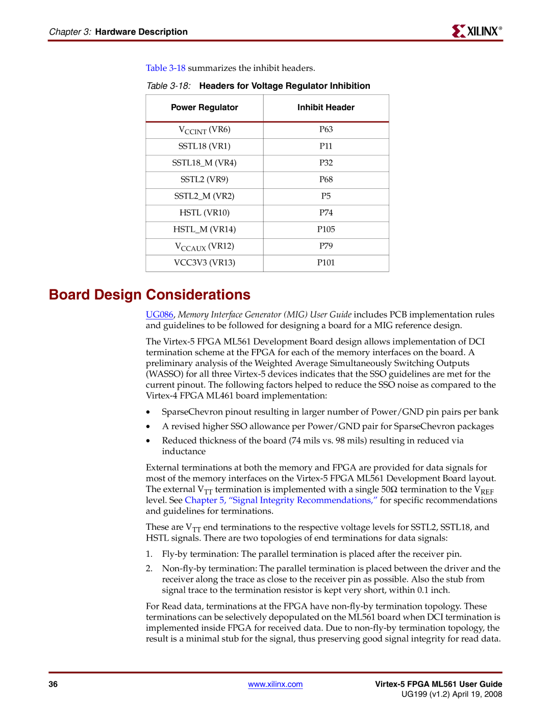
UG086, Memory Interface Generator (MIG) User Guide includes PCB implementation rules and guidelines to be followed for designing a board for a MIG reference design.
The Virtex-5 FPGA ML561 Development Board design allows implementation of DCI termination scheme at the FPGA for each of the memory interfaces on the board. A preliminary analysis of the Weighted Average Simultaneously Switching Outputs (WASSO) for all three Virtex-5 devices indicates that the SSO guidelines are met for the current pinout. The following factors helped to reduce the SSO noise as compared to the Virtex-4 FPGA ML461 board implementation:
•SparseChevron pinout resulting in larger number of Power/GND pin pairs per bank
•A revised higher SSO allowance per Power/GND pair for SparseChevron packages
•Reduced thickness of the board (74 mils vs. 98 mils) resulting in reduced via inductance
External terminations at both the memory and FPGA are provided for data signals for most of the memory interfaces on the Virtex-5 FPGA ML561 Development Board layout. The external VTT termination is implemented with a single 50Ω termination to the VREF level. See Chapter 5, “Signal Integrity Recommendations,” for specific recommendations and guidelines for terminations.
These are VTT end terminations to the respective voltage levels for SSTL2, SSTL18, and HSTL signals. There are two topologies of end terminations for data signals:
1.Fly-by termination: The parallel termination is placed after the receiver pin.
2.Non-fly-by termination: The parallel termination is placed between the driver and the receiver along the trace as close to the receiver pin as possible. Also the stub from signal trace to the termination resistor is kept very short, within 0.1 inch.
For Read data, terminations at the FPGA have non-fly-by termination topology. These terminations can be selectively depopulated on the ML561 board when DCI termination is implemented inside FPGA for received data. Due to non-fly-by termination topology, the result is a minimal stub for the signal, thus preserving good signal integrity for read data.
36 | www.xilinx.com | Virtex-5 FPGA ML561 User Guide |
| | UG199 (v1.2) April 19, 2008 |