R
Summary and Recommendations
Summary and Recommendations
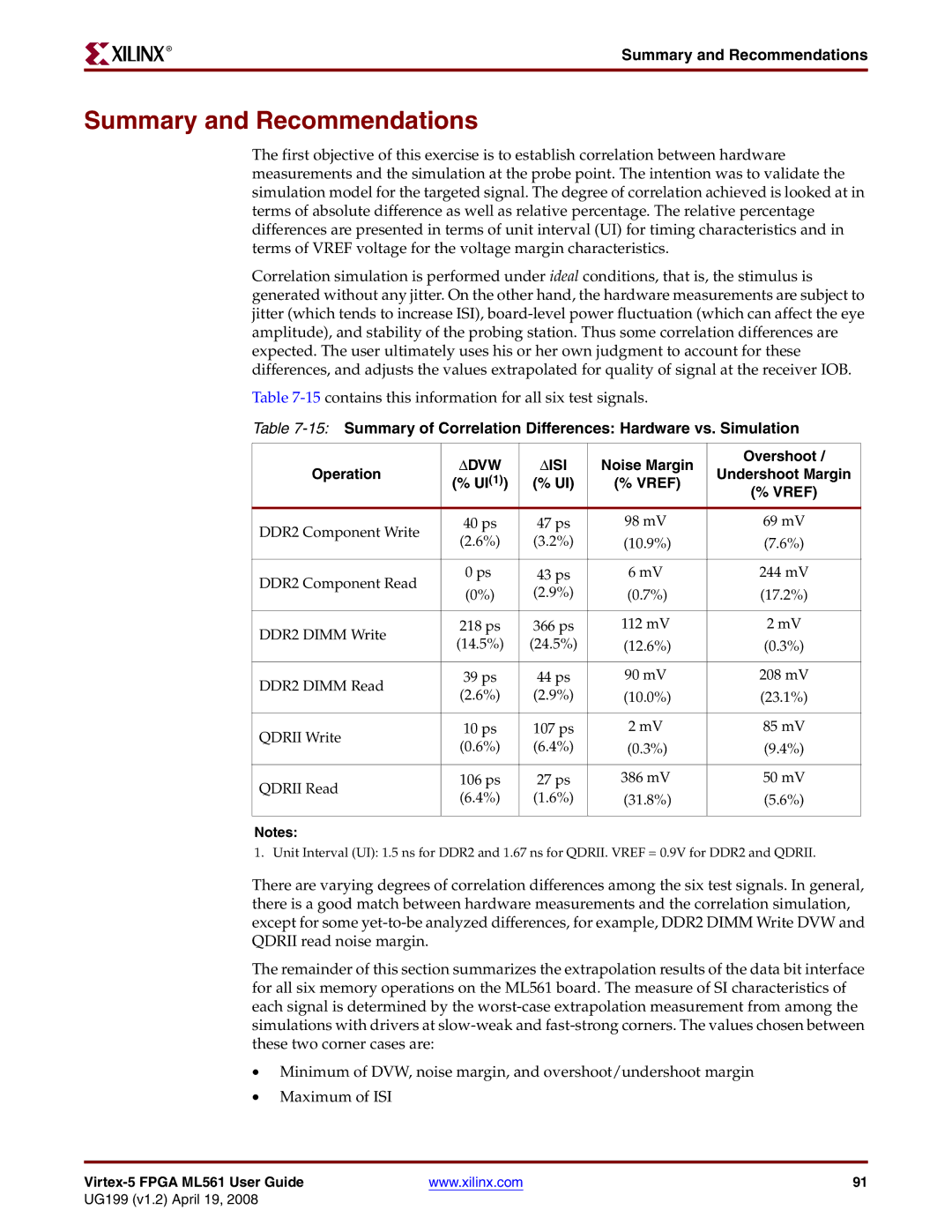
The first objective of this exercise is to establish correlation between hardware measurements and the simulation at the probe point. The intention was to validate the simulation model for the targeted signal. The degree of correlation achieved is looked at in terms of absolute difference as well as relative percentage. The relative percentage differences are presented in terms of unit interval (UI) for timing characteristics and in terms of VREF voltage for the voltage margin characteristics.
Correlation simulation is performed under ideal conditions, that is, the stimulus is generated without any jitter. On the other hand, the hardware measurements are subject to jitter (which tends to increase ISI),
Table
Table
| ΔDVW | ΔISI | Noise Margin | Overshoot / | |
Operation | Undershoot Margin | ||||
(% UI(1)) | (% UI) | (% VREF) | |||
| (% VREF) | ||||
|
|
|
| ||
|
|
|
|
| |
DDR2 Component Write | 40 ps | 47 ps | 98 mV | 69 mV | |
(2.6%) | (3.2%) | (10.9%) | (7.6%) | ||
| |||||
|
|
|
|
| |
DDR2 Component Read | 0 ps | 43 ps | 6 mV | 244 mV | |
(0%) | (2.9%) | (0.7%) | (17.2%) | ||
| |||||
|
|
|
|
| |
DDR2 DIMM Write | 218 ps | 366 ps | 112 mV | 2 mV | |
(14.5%) | (24.5%) | (12.6%) | (0.3%) | ||
| |||||
|
|
|
|
| |
DDR2 DIMM Read | 39 ps | 44 ps | 90 mV | 208 mV | |
(2.6%) | (2.9%) | (10.0%) | (23.1%) | ||
| |||||
|
|
|
|
| |
QDRII Write | 10 ps | 107 ps | 2 mV | 85 mV | |
(0.6%) | (6.4%) | (0.3%) | (9.4%) | ||
| |||||
|
|
|
|
| |
QDRII Read | 106 ps | 27 ps | 386 mV | 50 mV | |
(6.4%) | (1.6%) | (31.8%) | (5.6%) | ||
| |||||
|
|
|
|
|
Notes:
1. Unit Interval (UI): 1.5 ns for DDR2 and 1.67 ns for QDRII. VREF = 0.9V for DDR2 and QDRII.
There are varying degrees of correlation differences among the six test signals. In general, there is a good match between hardware measurements and the correlation simulation, except for some
The remainder of this section summarizes the extrapolation results of the data bit interface for all six memory operations on the ML561 board. The measure of SI characteristics of each signal is determined by the
•Minimum of DVW, noise margin, and overshoot/undershoot margin
•Maximum of ISI
| www.xilinx.com | 91 |
UG199 (v1.2) April 19, 2008