Chapter 3: Hardware Description
R
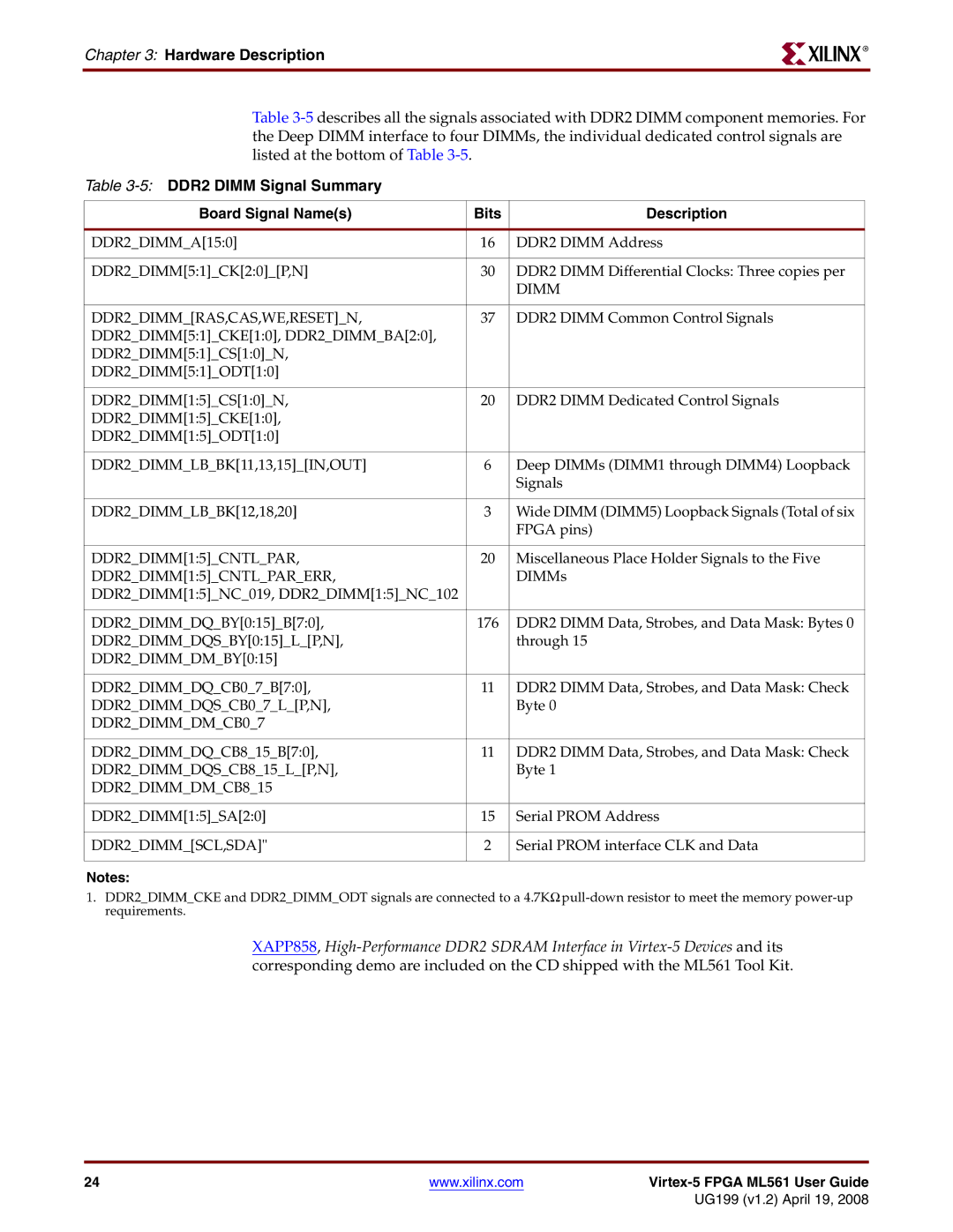
Table
Table
Board Signal Name(s) | Bits | Description |
|
|
|
DDR2_DIMM_A[15:0] | 16 | DDR2 DIMM Address |
|
|
|
DDR2_DIMM[5:1]_CK[2:0]_[P,N] | 30 | DDR2 DIMM Differential Clocks: Three copies per |
|
| DIMM |
|
|
|
DDR2_DIMM_[RAS,CAS,WE,RESET]_N, | 37 | DDR2 DIMM Common Control Signals |
DDR2_DIMM[5:1]_CKE[1:0], DDR2_DIMM_BA[2:0], |
|
|
DDR2_DIMM[5:1]_CS[1:0]_N, |
|
|
DDR2_DIMM[5:1]_ODT[1:0] |
|
|
|
|
|
DDR2_DIMM[1:5]_CS[1:0]_N, | 20 | DDR2 DIMM Dedicated Control Signals |
DDR2_DIMM[1:5]_CKE[1:0], |
|
|
DDR2_DIMM[1:5]_ODT[1:0] |
|
|
|
|
|
DDR2_DIMM_LB_BK[11,13,15]_[IN,OUT] | 6 | Deep DIMMs (DIMM1 through DIMM4) Loopback |
|
| Signals |
|
|
|
DDR2_DIMM_LB_BK[12,18,20] | 3 | Wide DIMM (DIMM5) Loopback Signals (Total of six |
|
| FPGA pins) |
|
|
|
DDR2_DIMM[1:5]_CNTL_PAR, | 20 | Miscellaneous Place Holder Signals to the Five |
DDR2_DIMM[1:5]_CNTL_PAR_ERR, |
| DIMMs |
DDR2_DIMM[1:5]_NC_019, DDR2_DIMM[1:5]_NC_102 |
|
|
|
|
|
DDR2_DIMM_DQ_BY[0:15]_B[7:0], | 176 | DDR2 DIMM Data, Strobes, and Data Mask: Bytes 0 |
DDR2_DIMM_DQS_BY[0:15]_L_[P,N], |
| through 15 |
DDR2_DIMM_DM_BY[0:15] |
|
|
|
|
|
DDR2_DIMM_DQ_CB0_7_B[7:0], | 11 | DDR2 DIMM Data, Strobes, and Data Mask: Check |
DDR2_DIMM_DQS_CB0_7_L_[P,N], |
| Byte 0 |
DDR2_DIMM_DM_CB0_7 |
|
|
|
|
|
DDR2_DIMM_DQ_CB8_15_B[7:0], | 11 | DDR2 DIMM Data, Strobes, and Data Mask: Check |
DDR2_DIMM_DQS_CB8_15_L_[P,N], |
| Byte 1 |
DDR2_DIMM_DM_CB8_15 |
|
|
|
|
|
DDR2_DIMM[1:5]_SA[2:0] | 15 | Serial PROM Address |
|
|
|
DDR2_DIMM_[SCL,SDA]" | 2 | Serial PROM interface CLK and Data |
|
|
|
Notes:
1.DDR2_DIMM_CKE and DDR2_DIMM_ODT signals are connected to a 4.7KΩ
XAPP858,
24 | www.xilinx.com |
|
|
| UG199 (v1.2) April 19, 2008 |