S3F80JB
Important Notice
Reset
Part Programming Model
Table of Contents
Interrupt Structure
Reset
Summary Table of Back-Up Mode, Stop Mode, and Reset Status
10-2
Timer
10-1
10-3
15-3
Flash Memory User Programming Enable Register Fmusr 15-6
15-1
15-5
List of Figures
Title Number
10-8
10-5
10-7
10-9
12-2
17-3 Typical Low-Side Driver Sink Characteristics
17-6 Typical High-Side Driver Source Characteristics
12-5
18-2
18-3 Typical Low-Side Driver Sink Characteristics
18-6 Typical High-Side Driver Source Characteristics
18-4
Reset Condition in Stop Mode When Ipor / LVD Control Bit is
List of Tables
17-13
17-3
17-6
18-3
Description
Chapter Reset
Chapter Basic Timer and Timer
Chapter Address Spaces
Register Full Register Name Identifier
Instruction Full Register Name Mnemonic
POP
Next
NOP
Popud
S3C8/S3F8-SERIES Microcontrollers
S3F80JB Microcontroller
Features
CPU
Block Diagram 32-PIN Package
Block Diagram 32-pin
Block Diagram 44-PIN Package
Block Diagram 44-pin
Pin Assignment Diagram 32-Pin SOP Package
PIN Assignments
44-QFP
PIN Assignments
S3F80JB
Pin Descriptions of 32-SOP Circuit 32 Pin Shared Names
Pin Descriptions of 44-QFP Circuit 44 Pin Shared Names
P3.1 Port with bit-programmable pin. Configurable to
PIN Circuits
Pin Circuit Type 1 Port 0 and Port2
PIN Circuits
Pin Circuit Type 2 Port 1, Port4, P3.4 and P3.5
Pin Circuit Type 3 P3.0
Pin Circuit Type 4 P3.1
10. Pin Circuit Type 6 nRESET
Address Space
Overview
Program Memory
Program Memory Address Space
Smart Option
Smart Option
S3F80JB Address Spaces
Total Addressable Bytes 333
Register Architecture
Summary of S3F80JB Register Type Number of Bytes
Internal Register File Organization
Register page Pointer PP
Register Page Pointer PP
Register SET
Prime Register Space
Set 1, Set 2, and Prime Area Register Map
Working Registers
Byte Working Register Areas Slices
Using the Register Pointers
Programming TIP Setting the Register Pointers
R0,R2
#80H RP0 ← 80H
R0,R1 ← R0 +
R0,R3
Register Addressing
Bit Register Pair
10. Register File Addressing
Common Working Register Area C0H-CFH
RP1 → C8H-CFH
BIT Working Register Addressing
Programming TIP Addressing the Common Working Register Area
Example
12 -Bit Working Register Addressing
14 -Bit Working Register Addressing
15 -Bit Working Register Addressing Example
Stack Pointers SPL
System and User Stacks
Stack Operations
Push RP1
SPL,#0FFH SPL ← FFH
Push RP0
POP RP1
Addressing Modes
Register Addressing Mode R
Register Addressing
Indirect Register Addressing Mode IR
Indirect Register Addressing to Register File
Indirect Register Addressing Mode
Indirect Register Addressing to Program Memory
Indirect Working Register Addressing to Register File
LCD
Indexed Addressing Mode
Indexed Addressing to Register File
Indexed Addressing Mode
Next 2 Bits
Indexed Addressing to Program or Data Memory
Direct Address Mode DA
10. Direct Addressing for Load Instructions
Direct Address Mode
11. Direct Addressing for Call and Jump Instructions
Indirect Address Mode IA
12. Indirect Addressing
Relative Address Mode RA
13. Relative Addressing
Immediate Mode IM
14. Immediate Addressing
Control Registers
T0DATA
T0CNT
D0H
D1H
Mapped Registers Register Name Mnemonic Decimal Hex
Register Description Format
Watchdog Timer Function Enable Bits for System Reset
Btcon Basic Timer Control Register D3H Set1 Bank0
Bit Identifier Reset Value Read/Write Addressing Mode
Basic Timer Input Clock Selection Bits
Cacon Counter a Control Register F3H Set1 Bank0
Subsystem Clock Selection Bits
Clkcon System Clock Control Register D4H Set1 Bank0
CPU Clock System Clock Selection Bits
Conversion Timer Control Bit
Cmod Comparator Mode Register E9H Set1 Bank1
Comparator Enable Bit
External Reference Selection Bit
P2.6 Function Selection Bit
Cmpsel Comparator Input Selection Register EBH Set1 Bank1
P2.7 Function Selection Bit
P2.5 Function Selection Bit
EMT External Memory Timing Register Note FEH Set1 Bank0
Flags System Flags Register D5H Set1 Bank0
Operation stop Operation start auto clear bit
Flash Memory Mode Selection Bits
Fmcon Flash Memory Control Register EFH Set1 Bank1
Flash Memory Sector Address Low Byte
Flash Memory User Programming Enable Bits
Flash Memory Sector Address High Byte
Interrupt Level 1 IRQ1 Enable Bit Timer 1 Match or Overflow
Interrupt Level 3 IRQ3 Enable Bit Timer 2 Match or Overflow
Interrupt Level 2 IRQ2 Enable Bit Counter a Interrupt
Interrupt Level 0 IRQ0 Enable Bit Timer 0 Match or Overflow
Instruction Pointer Address High Byte
IPH Instruction Pointer High Byte DAH Set1 Bank0
IPL Instruction Pointer Low Byte DBH Set1 Bank0
Instruction Pointer Address Low Byte
IPR Interrupt Priority Register FFH Set1 Bank0
Not pending
IRQ Interrupt Request Register DCH Set1 Bank0
Not pending Pending
Level 2 IRQ2 Request Pending Bit Counter a Interrupt
VDD ≥ Lvdflag Level VDD Lvdflag Level
LVD Flag 2.3V Indicator Bit
Lvdcon LVD Control Register E0H Set1 Bank1
P0.5/INT4 Mode Selection Bits
P0.7/INT4 Mode Selection Bits
P0.6/INT4 Mode Selection Bits
P0.4/INT4 Mode Selection Bits
P0.1/INT1 Mode Selection Bits
P0.3/INT3 Mode Selection Bits
P0.2/INT2 Mode Selection Bits
P0.0/INT0 Mode Selection Bits
P0.5 External Interrupt INT4 Enable Bit
P0.7 External Interrupt INT4 Enable Bit
P0.6 External Interrupt INT4 Enable Bit
P0.4 External Interrupt INT4 Enable Bit
P0.5 External Interrupt INT4 Pending Flag Bit
P0.7 External Interrupt INT4 Pending Flag Bit see Note
P0.6 External Interrupt INT4 Pending Flag Bit
P0.4 External Interrupt INT4 Pending Flag Bit
P0.5 Pull-up Resistor Enable Bit
P0.7 Pull-up Resistor Enable Bit
P0.6 Pull-up Resistor Enable Bit
P0.4 Pull-up Resistor Enable Bit
P1.5 Mode Selection Bits
P1.7 Mode Selection Bits
P1.6 Mode Selection Bits
P1.4 Mode Selection Bits
P1.1 Mode Selection Bits
P1.3 Mode Selection Bits
P1.2 Mode Selection Bits
P1.0 Mode Selection Bits
P2.5/INT9 Mode Selection Bits
P2.7/INT9 Mode Selection Bits
P2.6/INT9 Mode Selection Bits
P2.4/INT9 Mode Selection Bits
P2.1/INT6 Mode Selection Bits
P2.3/INT8 Mode Selection Bits
P2.2/INT7 Mode Selection Bits
P2.0/INT5 Mode Selection Bits
P2.5 External Interrupt INT9 Enable Bit
P2.7 External Interrupt INT9 Enable Bit
P2.6 External Interrupt INT9 Enable Bit
P2.4 External Interrupt INT9 Enable Bit
P2.5 External Interrupt INT9 Pending Flag Bit
P2.7 External Interrupt INT9 Pending Flag Bit see Note
P2.6 External Interrupt INT9 Pending Flag Bit
P2.4 External Interrupt INT9 Pending Flag Bit
P2.5 Pull-up Resistor Enable Bit
P2.7 Pull-up Resistor Enable Bit
P2.6 Pull-up Resistor Enable Bit
P2.4 Pull-up Resistor Enable Bit
P3CON Port 3 Control Register EFH Set1 Bank0
P3CON
Each Function Description and Assignment to P3.0-P3.3
P345CON Port345 Control Register E1H Set1 Bank1
P3.5 Mode Selection Bits
P3.4 Mode Selection Bits
Port 4 Control Register Selection Bit
P4CON Port 4 Control Register F0H Set1 Bank0
P4.5 Mode Selection Bits
P4.7 Mode Selection Bits
P4.6 Mode Selection Bits
P4.4 Mode Selection Bits
P4.1 Mode Selection Bits
P4.3 Mode Selection Bits
P4.2 Mode Selection Bits
P4.0 Mode Selection Bits
Source Register Page Selection Bits
PP Register Page Pointer DFH Set1 Bank0
Destination page 0 See Note
Source page 0 See Note
Register Pointer 0 Address Value
RP0 Register Pointer D6H Set1 Bank0
RP1 Register Pointer D7H Set1 Bank0
Register Pointer 1 Address Value
Stopcon Stop Control Register FBH Set1 Bank0
Stop Control Register Enable Bits
SPL Stack Pointer Low Byte D9H Set1 Bank0
Stack Pointer Address Low Byte
Global Interrupt Enable Bit
SYM System Mode Register DEH Set1 Bank0
Fast Interrupt Enable Bit
Tri-State External Interface Control Bit
T0CON- Timer 0 Control Register D2H Set 1 Bank0
T1CON Timer 1 Control Register FAH Set1 Bank0
T2CON Timer 2 Control Register E8H Set1 Bank1
Sources
Levels
Vectors
Interrupt Types
S3C8/S3F8-Series Interrupt Types
S3F80JB Interrupt Structure
S3F80JB Interrupt Structure
Interrupt Vector Addresses
ROM Vector Address Area
D8H
Interrupt Priority
FCH
Interrupt Control Register Overview Function Description
ENABLE/DISABLE Interrupt Instructions EI, DI
SYSTEM-LEVEL Interrupt Control Registers
Interrupt Function Diagram
Interrupt Processing Control Points
Peripheral Interrupt Control Registers
System Mode Register SYM
System Mode Register SYM
Interrupt Mask Register IMR
Interrupt Mask Register IMR
Interrupt Priority Register IPR
Interrupt Request Priority Groups
Interrupt Priority Register IPR
Interrupt Request Register IRQ
Interrupt Request Register IRQ
Overview
Pending Bits Cleared by the Service Routine
Interrupt Pending Function Types
Pending Bits Cleared Automatically by Hardware
Interrupt Service Routines
Interrupt Source Polling Sequence
Instruction Pointer IP
Generating Interrupt Vector Addresses
Nesting of Vectored Interrupts
Fast Interrupt Processing
Fast Interrupt Processing
Procedure for Initiating Fast Interrupt
Fast Interrupt Service Routine
Programming Guidelines
Data Types
Addressing Modes
Lded
LDE
LDC
Ldcd
Logic Instructions
Bit Manipulation Instructions
CPU Control Instructions
Flags Register Flags
System Flags Register Flags
Flag Descriptions
Flag Notation Conventions
Instruction Set Symbols
Instruction SET Notation
@Rn or @reg reg = 0-255, n =
Immediate addressing mode #data data =
Immediate long addressing mode #data data = range
Irr Indirect working register pair only @RRp p = 0, 2
Opcode Quick Reference
Opcode MAP Lower Nibble HEX
R1,IM
Djnz INC Next
R1,R2 R2,R1
Djnz INC NOP
Condition Codes
Condition Codes Binary Mnemonic Description Flags Set
Instruction Descriptions
Format Bytes Cycles
ADC Add with carry
Flags
Dst Src
ADD Add
Always cleared to
Logical
Flags Unaffected Set if the result is 0 cleared otherwise
Band Bit
Operation
BCP Bit Compare
BCP
Hex Dst
Bitc Bit Complement
Bitc
Format
Bitr Bit Reset
Bitr dst.b Operation dstb ←
Bits Bit Set
Bits dst.b Operation dstb ←
BOR Bit or
BOR
Btjrf SKIP,R1.3
Btjrf Bit Test, Jump Relative on False
Example Given R1 = 07H
Btjrt Bit Test, Jump Relative on True
Btjrt SKIP,R1.1
Bxor Bit XOR
R1,01H.1 R1 = 06H, register 01H = 03H
@SP PCL PCH
Call Call Procedure
Call
Operation C ← not C
CCF Complement Carry Flag
CCF
Complemented No other flags are affected
00H Register 00H
CLR Clear
CLR dst Operation dst ←
COM Complement
COM
CP Compare
INC Skip LD
Cpije Compare, Increment, and Jump on Equal
Cpije
If dst src 0, PC ← PC + RA
Cpijne Compare, Increment, and Jump on Non-Equal
Cpijne
Instruction
Bits
DA Decimal Adjust
DAdst Operation dst ← DA dst
3CH
R1,R0
R1 ← 3CH +
@R1 @R1 ← Leave the value 31 BCD in address 27H @R1
Dst Operation ← dst
DEC Decrement
DEC
Opc Dst Examples Given R1 = 03H and register 03H = 10H
Decw Decrement Word
Decw
No flags are affected
DI Disable Interrupts
Operation SYM 0 ←
DIV Divide Unsigned
Operation dst ÷ src
Jump taken No jump
Djnz Decrement and Jump if Non-Zero
Djnz r,dst Operation r ← r
SRP #0C0H Djnz R1,LOOP
EI Enable Interrupts
Operation SP
Enter Enter
Enter
@SP @IP
Operation IP
Exit Exit
Exit
@SP
Idle Idle Operation
Idle
INC dst Operation dst ← dst +
Contents of the destination operand are incremented by one
INC Increment
= 1CH
Incw RR0
Incw Increment Word
Incw
Loop Incw RR0
Flags ← @SP PC ↔ IP
Iret Interrupt Return
Iret
Flags ← Flags
JP Jump
Labelw
Labelx → PC = 1FF7H
JR Jump Relative
Example Given The carry flag = 1 and Labelx = 1FF7H
LD Load
Dst ← src
Register 31H = 0AH, R0 = 01H, R1 = 0AH
0AH
= 0FFH, R1 = 0AH
Dst Examples Given R0 = 06H and general register 00H = 05H
LDB Load Bit
LDB
R0,00H.2 07H, register 00H 05H
LDC/LDE dst,src Operation dst ← src
Addr Mode
LDC/LDE Load Memory
XL L XL H
LDC/LDE
Examples
LDCD/LDED Load Memory and Decrement
LDCD/LDED dst,src Operation dst ← src
Rr ← rr +
LDCI/LDEI Load Memory and Increment
LDCI/LDEI dst,src Operation dst ← src
Into R8 and RR6 is incremented by one RR6 ← RR6 +
Operation rr ← rr
LDCPD/LDEPD Load Memory with Pre-Decrement
Ldcpd
Operation rr ← rr +
LDCPI/LDEPI Load Memory with Pre-Increment
Ldcpi
LDW RR6,RR4
LDW Load Word
RR IML
Operation dst ← dst ⋅ src
Mult Multiply Unsigned
Mult dst,src
Cleared
Operation PC ← @ IP
Next Next
Next
NOP
When the instruction
NOP No Operation
Or Logical or
00H Register 00H 55H, SP = 00FCH
POP Pop From Stack
POP dst Operation dst ← @SP
Popud Pop User Stack Decrementing
Popud dst,src
Popui Pop User Stack Incrementing
Popui dst,src
SPH = 0FFH, SPL = 0FFH
Push Push To Stack
Push src Operation SP ← SP
0FFH = 0AAH, SPH = 0FFH, SPL = 0FFH
IR ← IR
Pushud Push User Stack Decrementing
Pushud
Decremented stack pointer
Pushui Push User Stack Incrementing
Pushui dst,src Operation IR ← IR +
Flags Cleared to
RCF Reset Carry Flag
RCF
Operation PC ← @SP
RET Return
RET
PC = 101AH, SP = 00FEH
Dst n + 1 ← dst n, n =
RL Rotate Left
Dst 0 ← dst
Set if the result bit 7 is set cleared otherwise
RLC Rotate Left Through Carry
RLC
Operation C ← dst
RR Rotate Right
RR dst
Rotation cleared otherwise
Dst 7 ← C
RRC Rotate Right Through Carry
RRC
00H Register 00H 2AH, C =
Operation Bank ←
SB0 Select Bank
SB0
Statement
SB1 Select Bank
SB1
Set otherwise, indicating a borrow Format Bytes Cycles
SBC Subtract With Carry
Always set to
Set to No other flags are affected
SCF Set Carry Flag
SCF
Sets the carry flag to logic one
00H Register 00H 0CD, C =
SRA Shift Right Arithmetic
SRA dst
SRP0
SRP/SRP0/SRP1 Set Register Pointer
SRP
SRP1
Stop Stop Operation
Stop
Set otherwise indicating a borrow Format Bytes Cycles
SUB Subtract
SUB
Flags Undefined Set if the result is 0 cleared otherwise
Swap Swap Nibbles
Swap dst
00H Register 00H 0E3H
R0,@R1 = 0C7H, R1 = 02H, register 02H = 23H, Z =
TCM Test Complement Under Mask
R0,R1 = 0C7H, R1 = 02H, Z =
00H,01H Register 00H = 2BH, register 01H = 02H, Z =
TMdst,src
Always reset to
TM Test Under Mask
Operation dst and src
Opc 4n 3F
WFI Wait For Interrupt
WFI
7FH
XOR Logical Exclusive or
XOR
Clock Circuits
System Clock Circuit
Clock Status During POWER-DOWN Modes
System Clock Circuit Diagram
System Clock Control Register Clkcon
System Clock Control Register Clkcon
Reset
Reset Sources
EIexternal interrupt enable
Reset Sources of The S3F80JB
Reset Block Diagram of The S3F80JB
Watch DOG Timer Reset
Reset Mechanism
External Reset PIN
LVD Reset
Internal POWER-ON Reset
Internal Power-On Reset Circuit
Timing Diagram for Internal Power-On Reset Circuit
Reset Timing Diagram for The S3F80JB in Stop mode by Ipor
External Interrupt Reset
Reset Source
Stop Error Detection & Recovery
Vreset
Slope of V DD
Idle Mode Release
POWER-DOWN Modes
Idle Mode
BACK-UP Mode
Block Diagram for Back-up Mode
Stop Mode
Programming TIP To Enter Stop Mode
Using Ipor to Release Stop Mode
Sources to Release Stop Mode
Using nRESET Pin to Release Stop Mode
Using LVD to Release Stop Mode
SED&R Stop Error Detect and Recovery
System Reset Operation
Hardware Reset Values
Dec
Timer 1 Control Register
Timer 1 Data Register High Byte
Timer 1 Data Register Low Byte
Dec Hex
Timer 2 Data Register Low Byte
Timer 2 Counter Register Low Byte
Timer 2 Data Register High Byte
Timer 2 Control Register
Stop Ipor
Ipor
LVD
SED&R
P2PUR
Recommendation for Unusued Pins
← # 0FFH
Connect to VSS
Stopcon ← # A5H
Summary Table of BACK-UP MODE, Stop MODE, and Reset Status
Summary of Each Mode Item/Mode Back-up Reset Status Stop
LD STOPCON,#0A5H
O Ports
Assigned individually as analog input pin for comparator
S3F80JB Port Configuration Overview 44-QFP
Port Configuration Options
P3.0-P3.1
S3F80JB Port Configuration Overview 32-SOP
Port Data Registers
S3F80JB I/O Port Data Register Format
PULL-UP Resistor Enable Registers
Pull-up Resistor Enable Registers Port 0 and Port 2 only
Basic Timer BT
Timer
Basic Timer Control Register Btcon
Basic Timer Control Register Btcon
Oscillation Stabilization Interval Timer Function
Basic Timer Function Description
Watch-dog Timer Function
Timer 0 Control Register T0CON
Timer 0 Control Register T0CON
Interval Timer Mode
Timer 0 Function Description
Timer 0 Interrupts IRQ0, Vectors FAH and FCH
Pulse Width Modulation Mode
Simplified Timer 0 Function Diagram PWM Mode
Capture Mode
Simplified Timer 0 Function Diagram Capture Mode
Basic Timer and Timer 0 Block Diagram
CLR SPL
Programming TIP Configuring the Basic Timer
CLR SYM
Main BTCON,#52H
Programming TIP Programming Timer
T0OVER Iret
ULT,NO200MSSET Bits
NO200MSSET
Timer
Timer 1 Overflow Interrupt
Timer 1 Capture Interrupt
Timer 1 Match Interrupt
Simplified Timer 1 Function Diagram Interval Timer Mode
Timer 1 Block Diagram
Timer 1 Control Register T1CON
Timer 1 Control Register T1CON
Timer 1 Registers T1CNTH, T1CNTL, T1DATAH, T1DATAL
Counter a
Counter a Block Diagram
Counter a Control Register Cacon
Counter a Control Register Cacon
Method 2 When Caof =
Counter a Pulse Width Calculations
Counter a Output Flip-Flop Waveforms in Repeat Mode
Through P3.1
CADATAL,#
Programming TIP To generate a one-pulse signal through P3.1
CADATAH,# Set 40 ms
Set any value except 00H
13-1
Timer 2 Overflow Interrupt
Timer 2 Capture Interrupt
Timer 2 Match Interrupt
Simplified Timer 2 Function Diagram Interval Timer Mode
Timer 2 Block Diagram
Timer 2 Control Register T2CON
Timer 2 Control Register T2CON
Timer 2 Registers T2CNTH, T2CNTL, T2DATAH, T2DATAL
Comparator
Comparator Block Diagram for The S3F80JB
Conversion Characteristics
Comparator Operation
Comparator Mode Register Cmod
Comparator Result Register Cmpreg
Flash ROM Configuration
Embedded Flash Memory Interface
Pin No Function
User Program Mode
Tool Program Mode
Isptm ON-BOARD Programming Sector
15-4
Area of ISP Sector ISP Sector Size
ISP Reset Vector and ISP Sector Size
ISP Sector Size
Bit
Flash Memory Control Register Fmcon
Flash Memory Control Registers User Program Mode
Flash Memory User Programming Enable Register Fmusr
Flash Memory Sector Address Registers
Flash Memory Sector Address Register Fmsech
Sector Configurations in User Program Mode
Sector Erase
Sector Erase Procedure in User Program Mode
Sector Erase Flowchart in User Program Mode
Programming TIP Sector Erase Case1. Erase one sector
Nocarry
Sectorerase
Btjrf FLAGS.7,NOCARRY
Erasestart SB1 FMUSR,#0A5H
Program procedure in user program mode
Programming
Byte Program Flowchart in a User Program Mode
10. Program Flowchart in a User Program Mode
Programming TIP Programming Case1 -Byte Programming
Case2. Programming in the same sector
Call Wrbyte
WRINSECTOR2
LD FMSECH,#01H
WRINSECTOR50 FMSECH,#19H
Loop LDC
Reading
Programming TIP Reading
NZ,LOOP
FMCON,#01100001B
Hard Lock Protection
Programming TIP Hard Lock Protection
LVD
LVD Flag
Resistor String
LOW Voltage Detector Control Register Lvdcon
Low Voltage Detect Control Register Lvdcon
Electrical Data 4MHz
Parameter Symbol Conditions Min Typ Max Unit
Parameter Symbol Conditions Rating Unit
D.C. Electrical Characteristics
Absolute Maximum Ratings
Vout = 0 Leakage Current All output pins Pull-Up
Leakage Current All input pins except ILIH2 and Xout
Leakage Current All output pins Output Low
Output Low
Data Retention Supply Voltage in Stop Mode
Characteristics of Low Voltage Detect Circuit
Parameter Symbol Conditions
Min Typ Max Unit
Typical Low-Side Driver Sink Characteristics P3.1 only
Typical High-Side Driver Source Characteristics P3.1 only
Typical VDD-VOHVDD=3.3V
Stop Mode Release Timing When Initiated by a Reset
A.C. Electrical Characteristics
10. Input Timing for External Interrupts Port 0 and Port
Oscillation Characteristics
Oscillator Clock Circuit Conditions Min Typ Max Unit
Oscillation Stabilization Time
When released by a reset 216/f Stabilization
Wait time TWAIT when released by an interrupt
TA = 25 C to + 85 C, VDD = 3.6
Chip Erasing Time
100 Data Access Time
Sector Erasing Time
VDD = 2.0 250 Number of Writing/Erasing FNwe 10,000
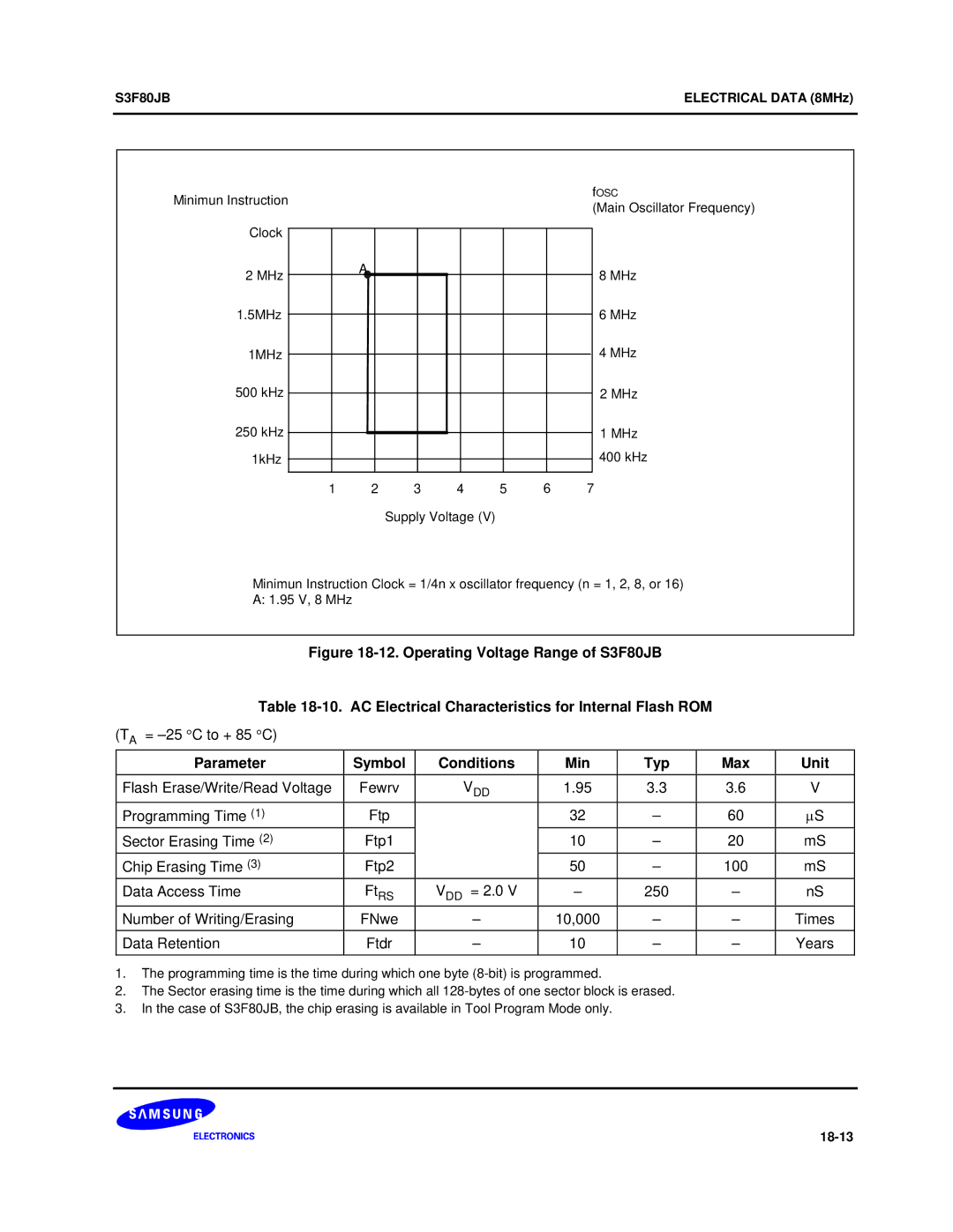
Electrical Data 8MHZ
VDD = 2.35 V, IOH = 6mA
TA = 25 C to + 85 C, VDD = 1.95 V to 3.6
Fosc = 8 MHz Input High Voltage
VDD = 2.35 V, IOH = 2.2mA P3.0 and P2.0-2.3
Leakage Current All output pins Pull-Up Resistors
Leakage Current All input pins except ILIH2
Leakage Current All input pins except ILIL2
VDD = 2.35 V, IOL = 12mA
Stop Mode LVD OFF, V DD = 3.6 LVD ON, V DD = 3.6
Operating Mode DD = 3.6 MHz crystal
Idle Mode DD =3.6 MHz crystal
For Back-Up Mode Low Level Detect Voltage
Vddv
Typical VDD-VOHVDD=3.3V
IOHmA
Typical VDD-VOHVDD=3.3V
VDD-VOHV
18-8
18-9
18-10
Comparator Electrical Characteristics
Parameter Symbol Condition Min Typ Max Units
TA = -25 C to + 85 C, VDD = 3.6
Flash Erase/Write/Read Voltage Fewrv
18-14
Pin SOP Package Dimension
SOP-450A
QFP-1010B
Target Boards
Programming Socket Adapter
TB80JB Target Board Configuration
TB80JB Target Board
VCC, GND, S
Components Consisting of S3F80JB Target Board Block Symbols
J1A
IDLE, Stop LED
Stop LED
JP#
Idle LED
Pin Connector Pin Assignment for TB80JB
GW-PRO2
Series In-Circuit Emulator
OTP/MTP Programmer
Development Tools Suppliers
GW-PRO2
OTP/MTP Programmer Writer SPW2+
Seminix
Package Marking Check One
For what kind of product will you be using this order?
Product description
Customer sample Risk order
Order Quantity and Delivery Schedule
Risk Order Information
Customer Risk Order Agreement
Delivery Date s Quantity Comments Signatures
Flash Application Notes
VDD
S3F80JB
Important Note
For Serial Programming Mode
S3F80JB/9 is needed to nRESET pin = 0GND & Test pin = 1VDD
When nRESET pin = 1VDD & Test pin = 0GND
For Normal Operating Mode
S3F80JB/9 is needed to nRESET pin = 1VDD & Test pin = 0GND
Timing Diagram
When Test PIN = 1VDD
¾ When S3F80JB
¾ When S3F80J9