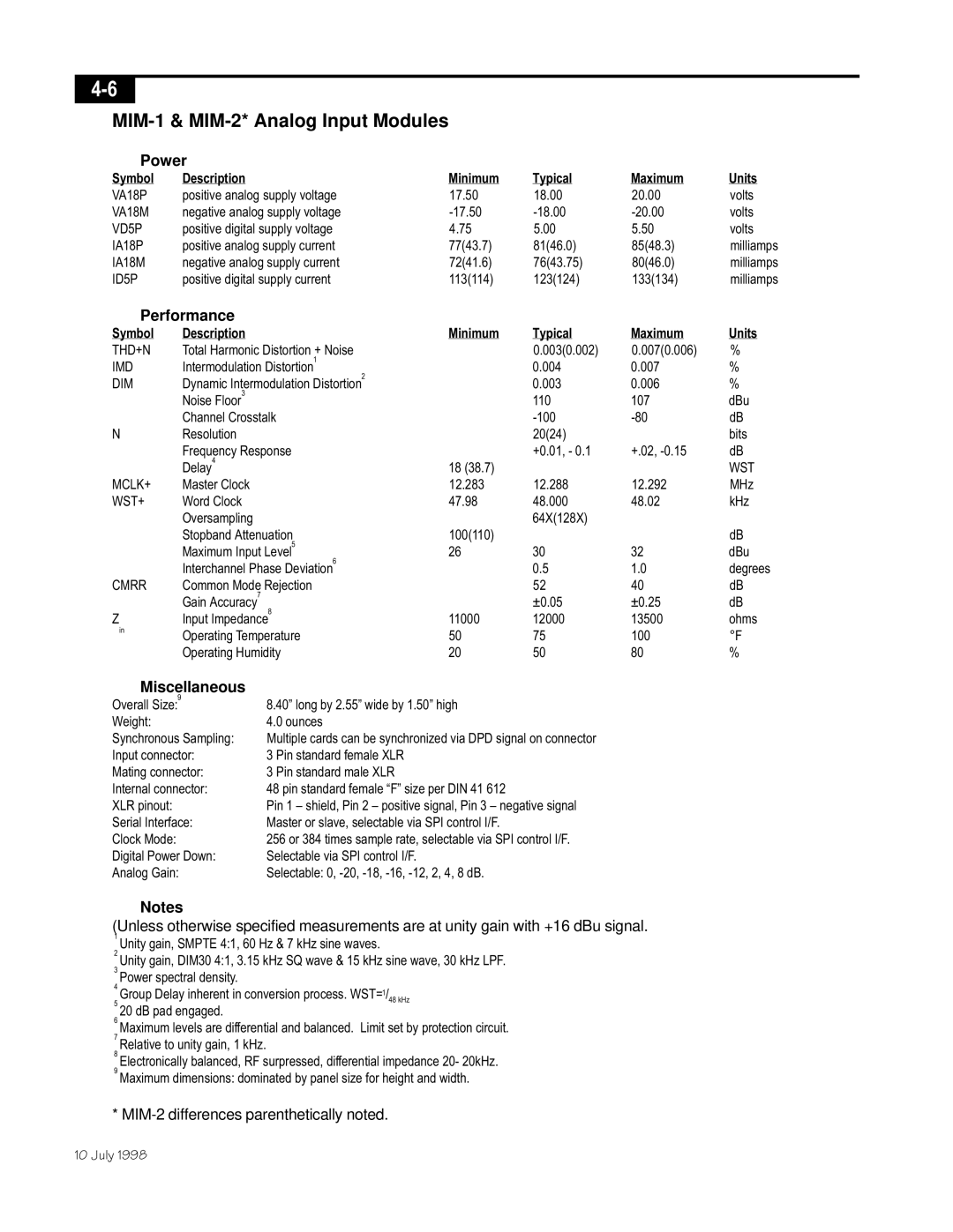
MIM-1 & MIM-2* Analog Input Modules
Power
Symbol | Description | Minimum | Typical | Maximum | Units |
VA18P | positive analog supply voltage | 17.50 | 18.00 | 20.00 | volts |
VA18M | negative analog supply voltage | volts | |||
VD5P | positive digital supply voltage | 4.75 | 5.00 | 5.50 | volts |
IA18P | positive analog supply current | 77(43.7) | 81(46.0) | 85(48.3) | milliamps |
IA18M | negative analog supply current | 72(41.6) | 76(43.75) | 80(46.0) | milliamps |
ID5P | positive digital supply current | 113(114) | 123(124) | 133(134) | milliamps |
Performance
Symbol | Description | Minimum | Typical | Maximum | Units |
THD+N | Total Harmonic Distortion + Noise |
| 0.003(0.002) | 0.007(0.006) | % |
IMD | Intermodulation Distortion1 |
| 0.004 | 0.007 | % |
DIM | Dynamic Intermodulation Distortion2 |
| 0.003 | 0.006 | % |
| Noise Floor3 |
| 110 | 107 | dBu |
| Channel Crosstalk |
| dB | ||
N | Resolution |
| 20(24) |
| bits |
| Frequency Response |
| +0.01, - 0.1 | +.02, | dB |
| Delay4 | 18 (38.7) |
|
| WST |
MCLK+ | Master Clock | 12.283 | 12.288 | 12.292 | MHz |
WST+ | Word Clock | 47.98 | 48.000 | 48.02 | kHz |
| Oversampling |
| 64X(128X) |
|
|
| Stopband Attenuation | 100(110) |
|
| dB |
| Maximum Input Level5 | 26 | 30 | 32 | dBu |
| Interchannel Phase Deviation6 |
| 0.5 | 1.0 | degrees |
CMRR | Common Mode Rejection |
| 52 | 40 | dB |
| Gain Accuracy7 |
| ±0.05 | ±0.25 | dB |
Z | Input Impedance8 | 11000 | 12000 | 13500 | ohms |
in | Operating Temperature | 50 | 75 | 100 | °F |
| |||||
| Operating Humidity | 20 | 50 | 80 | % |
Miscellaneous
Overall Size:9 | 8.40” long by 2.55” wide by 1.50” high |
Weight: | 4.0 ounces |
Synchronous Sampling: | Multiple cards can be synchronized via DPD signal on connector |
Input connector: | 3 Pin standard female XLR |
Mating connector: | 3 Pin standard male XLR |
Internal connector: | 48 pin standard female “F” size per DIN 41 612 |
XLR pinout: | Pin 1 – shield, Pin 2 – positive signal, Pin 3 – negative signal |
Serial Interface: | Master or slave, selectable via SPI control I/F. |
Clock Mode: | 256 or 384 times sample rate, selectable via SPI control I/F. |
Digital Power Down: | Selectable via SPI control I/F. |
Analog Gain: | Selectable: 0, |
Notes
(Unless otherwise specified measurements are at unity gain with +16 dBu signal.
1Unity gain, SMPTE 4:1, 60 Hz & 7 kHz sine waves.
2Unity gain, DIM30 4:1, 3.15 kHz SQ wave & 15 kHz sine wave, 30 kHz LPF.
3 Power spectral density.
4 Group Delay inherent in conversion process. WST=1/48 kHz 5 20 dB pad engaged.
6 Maximum levels are differential and balanced. Limit set by protection circuit. 7 Relative to unity gain, 1 kHz.
8 Electronically balanced, RF surpressed, differential impedance 20- 20kHz. 9 Maximum dimensions: dominated by panel size for height and width.
*
10 July 1998