Network Commprocessor
Attached System Bus LAN Subsystem
Pinout
PIN Quad Flat Pack TOP View
Description
Block diagram and signal descriptions
Terminal Functions
TMS380C26
PIN Name Description
Maxph
AX1 AX0
Maxpl
AX3 AX2
Sreset
Mreset OUT
MOE
Mras
Prtyen
NSELOUT0 NSELOUT1
= H
Sbhe
Shrq
Sddir Direction DIO DMA
Sintr
SRD
SWR
108 Reserved. This signal must be left unconnected see Note
= Selects 8-bit mode see Note
= Selects 16-bit mode
Syncin
= L
System Interface ± Motorola Mode SI/M
SBHE/ Srnw
Terminal Functions = L
Sbgr
Sbrq
Sirq
Sdtack
Suds
Slds
FRAQ/TXD
Nsrt
Pxtalin
RCVR/RXD
TXC
Lpbk
Coll
Terminal Functions
Vssl
VSS1 VSS2
VSS3
VSS4 VSS5 VSS6
Communications processor CP
Architecture
System interface SIF
Memory interface MIF
Protocol handler PH
Adapter support function ASF
Clock generator CG
Adapter-Internal Pointers for Token-Ring²
Address Description
Adapter-Internal Pointers for Ethernet ²
User-Access Hardware Registers
³ 68xxx Mode is always 16-bit
Word Transfers
Byte Transfers
Bits 0-2 Test 0±2. Value on Test 0±2 pins
Bit 5 Swddir Ð Current Sddir Signal Value
SIF Adapter Control Register Sifacl
Sifacl Register
Bit 6 Swhrq Ð Current Shrq Signal Value
Bit 7 Psdmaen Ð Pseudo-System-DMA Enable
Bit 8 Areset Ð Adapter Reset
Bit 10 Boot Ð Bootstrap CP Code
Bit 12 Sinten Ð System-Interrupt Enable
Bit 13 PEN Ð Adapter Parity Enable
Bit 14 Ð 15 Nselout 0±1 Ð Network selection outputs
System Psdmaen Swhrq Swhlda Sinten Interrupt Result
Sifacl Control for Pseudo-DMA Operation
Systeminterrupt SINTR/SIRQ
DMA SHRQ/SBRQ
Dmadir Sddir Swhlda Swddir Swhrq Psdmaen Sinten
Recommended operating conditions
MIN NOM MAX Unit
Parameter Test Conditions MIN TYP MAX Unit
See Note
Test measurement
High Low
Vload IOL
Output Under Test
When
Reference Periods
Clkdiv = Oscout MBCLK1² MBCLK2²
Static signals
Timing parameter symbology
Signal Function
Timing parameters
289² ThRST Hold time of DMA size from High Intel mode only
Parameter MIN MAX Unit
Reaches minimum high level
HVDDH-RSL 118² Pulse duration High
VDD Sbclk Oscin MBCLK1 MBCLK2 Sreset S8/SHALT
Minimun VDD High Level
103
101 106 104 105 102 107 110 108 109 111 117 118 119 288 289
126 Delay time from MBCLK1 no longer low to Valid
Mreset
NMI
121 Hold time Valid after MBCLK1 low
MBCLK1 MBCLK2 MAX0 MAX2 ADD/EN Mromen Maxph Maxpl
Mreset
MADH0±MADH7
MADL0±MADL7 Maxph Maxpl
Memory bus timing clocks, MRAS, MCAS, and MAL to Address
Mromen MAL
Column Row
Address
Address Status
Column Status
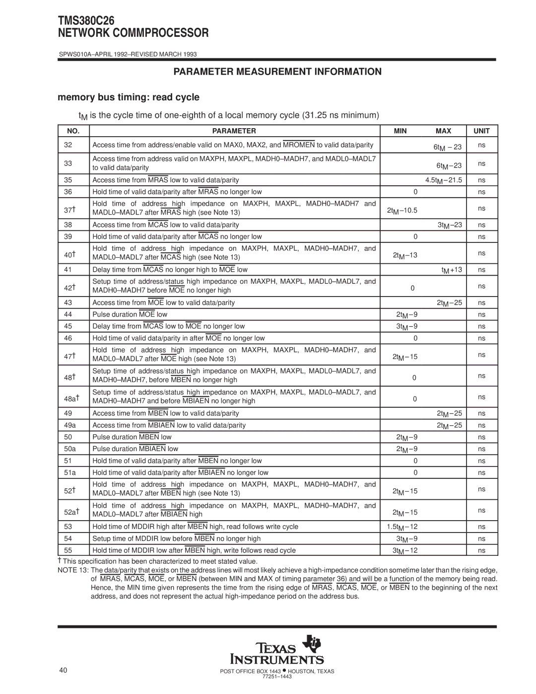
Memory bus timing read cycle
Mcas MOE
Maxph Maxpl MADH0±MADH7
Maxph Maxpl
MAX0 MAX2 Mromen
Mras Mcas
Address Status Data/Parity
Mbiaen
Memory bus timing write cycle
Enable Address
MAX0, Address
MAX2 Mromen
Mras Mcas Mben
Memory bus timing TMS380C26 releases control of bus
Parameter MIN
75a 74a
MBCLK1 MBCLK2 Mben
Mddir MAL Mbiaen Mbrq Mbgr
Memory bus timing TMS380C26 resumes control of bus
Setup time High before MBCLK1 rising edge, bus resume
Hold time Valid after MBCLK1 low, bus resume
Memory Bus Timing TMS380C26 Resumes Control of Bus
Mben Mddir MAL Mbiaen Mbrq Mbgr
Macs
Memory bus timing external bus master read from TMS380C26
Hold time Low after MBCLK2 low, external bus master read
MAX0 MAX2 Maxph Maxpl MADH0±MADH7
MBCLK1 MBCLK2
Mddir Macs
MAX0, MAX2 Maxph Maxpl
Memory bus timing external bus master write to TMS380C26
Data/Pty
Memory bus timing Dram refresh timing
MADL0±MADL7 Mras
73a
Mcas Mref
Xmatch and Xfail timing
Bit
127 128
Xmatch Xfail
Token ring Ð ring interface timing
Parameter MIN TYP MAX Unit
Rclk
Rcvr
Token ring Ð transmitter timing see Figure
Rclk or Pxtalin
Drvr
160 159
Ethernet timing of clock signals
Ethernet timing of Xmit signals
TXD
Txen
Ethernet timing of RCV signals Ð start of frame
CRS
RXC
RXD
Ethernet timing of RCV signals Ð end of frame
Crshld
320 321
322
Norxc
Ethernet timing of RCV signals Ð no RXC
TXD Txen
350
TXC TXD
Data
JAM
80x8x DIO read timing
SCS, Srsx
SRS0± SRS2 Sbhe
Sras
Sdben
80x8x DIO write timing
Valid 264 265 268 256
267 272a 280 281
281a
282W 283W 276 279 275 282b
80x8x interrupt acknowledge timing ± first Siack pulse
80x8x interrupt acknowledge timing ± second Siack pulse
SRD, SWR SCS Siack
287 First 286 Second
SCS, Srsx SRS0±SRS2 Sbhe Siack SWR SRD
Sddir High
Sdben SRDY²HI-Z
SADH0±SADH7 SADL0±SADL7,HI-ZSPH, SPL
80x8x mode bus arbitration timing, SIF takes control
Sown
SRD SWR
SWR Sown
SRD, SWR
Sbbsy Shlda
SADL0±SADL7 SPH, SPL
After Sbclk low to guarantee recognition on this cycle
212 Delay from Sbclk low to address valid 214 ²
This cycle 208b
High TwSCKL ±
Sbclk Sras
80x8x mode DMA write timing
Slds
SRD High
SADL0±SADH7
SADH0±SADL7 SPH, SPL
Sddir High
80x8x mode bus arbitration timing, SIF returns control
80x8x mode bus release timing
Sbrls Sown
TW or
208c
68xxx DIO read timing
SRS0, SRS1
Siack Srnw
Suds Slds
SDTACK²HI-Z SADH0±SADH7 SADL0±SADL7,HI-Z SPH, SPL
68xxx DIO write timing
Suds Slds Sdtack
SCS SRSX, SRS0, SRS1 Siack Srnw
SDBEN³
SDTACK²
SADH0±SADH7 SADL0±SADL7,HI-Z SPH, SPL
68xxx interrupt acknowledge cycle timing
SCS Siack
SCS Srnw Sdtack
Siack Sdtack
SCS, Srsx SRS0, SRS1 Sbhe Siack Srnw Slds
Sdben SDTACK² HI-Z
SADH0±SADH7 SADL0±SADL7, HI-ZSPH, SPL
275 282a 255
68xxx mode bus arbitration timing, SIF takes control
241 Delay from Sbclk high in TX cycle to High
Sbgr
Sbrq
Sberr Sdtack Sbbsy
SAS, Slds
Suds Srnw
SADH0±SADH7 HI-Z SADL0±SADL7 SPH, SPL
68xxx mode DMA read timing
237R Delay from Sbclk high in the T2 cycle to Low
On this cycle 208b
Suds SAS
Sale SADL0±SADH7 SADH0±SADL7 SPH, SPL
68xxx mode DMA write timing
Sdben Suds Slds
SAS
SADL0±SADH7, SADH0±SADL7 SPL, SPH
68xxx mode bus arbitration timing, SIF returns control
240 ² Setup SRNW,
Sbclk Sbgr Sdtack
Read HI-Z Write
SIF HI-Z
Write Read
68xxx mode bus release and error timing
Sown Sberr
Sbrls Sown
Sberr Sdtack
Rerun cycle with delayed start²
Normal completion with delayed start²
Sbclk Sdtack Sberr Shalt
TH B TH E Sbclk Sdtack Sberr Shalt Sown
Jedec plastic leaded quad flat package PQ suffix
254 0.010 NOM 635 0.025 NOM 76 0.030 NOM
Jedec NO. Outline Terminals MIN MAX
MO±069±AD
Important Notice