|
|
|
|
|
|
|
|
|
|
|
| TMS380C26 | |
|
|
|
|
|
|
|
|
|
|
| NETWORK COMMPROCESSOR | ||
|
|
|
|
|
|
|
|
|
|
| SPWS010A±APRIL 1992±REVISED MARCH 1993 | ||
|
|
|
|
|
|
|
|
|
|
|
|
| |
|
|
|
|
|
|
|
|
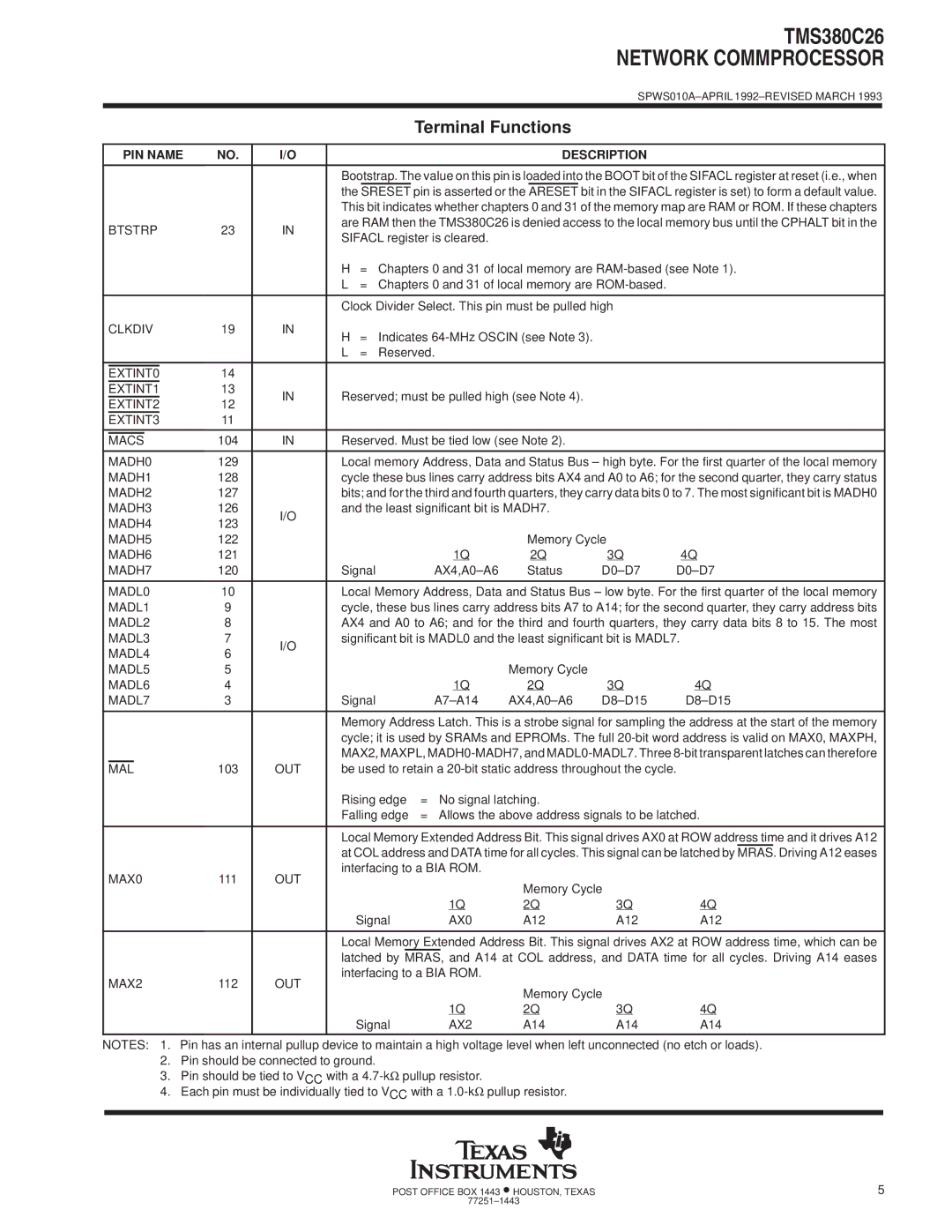
| Terminal Functions |
|
|
| |
|
|
|
|
|
|
|
|
|
|
|
|
| |
| PIN NAME | NO. | I/O |
|
|
| DESCRIPTION |
|
| ||||
|
|
|
|
|
|
|
| ||||||
|
|
|
|
|
|
| Bootstrap. The value on this pin is loaded into the BOOT bit of the SIFACL register at reset (i.e., when | ||||||
|
|
|
|
|
|
| the SRESET pin is asserted or the ARESET bit in the SIFACL register is set) to form a default value. | ||||||
|
|
|
|
|
|
| This bit indicates whether chapters 0 and 31 of the memory map are RAM or ROM. If these chapters | ||||||
| BTSTRP | 23 | IN | are RAM then the TMS380C26 is denied access to the local memory bus until the CPHALT bit in the | |||||||||
| SIFACL register is cleared. |
|
|
|
| ||||||||
|
|
|
|
|
|
|
|
|
|
| |||
|
|
|
|
|
|
| H | = Chapters 0 and 31 of local memory are | |||||
|
|
|
|
|
|
| L | = Chapters 0 and 31 of local memory are |
|
| |||
|
|
|
|
|
|
|
|
|
| ||||
|
|
|
|
|
|
| Clock Divider Select. This pin must be pulled high |
|
| ||||
| CLKDIV | 19 | IN | H | = Indicates |
|
|
| |||||
|
|
|
|
|
|
|
|
|
| ||||
|
|
|
|
|
|
| L | = Reserved. |
|
|
|
| |
|
|
|
|
|
|
|
|
|
|
|
|
| |
|
|
|
|
| 14 |
|
|
|
|
|
|
|
|
| EXTINT0 |
|
|
|
|
|
|
|
|
| |||
| EXTINT1 | 13 | IN | Reserved; must be pulled high (see Note 4). |
|
|
| ||||||
| EXTINT2 | 12 |
|
|
| ||||||||
|
|
|
|
|
|
|
|
| |||||
| EXTINT3 | 11 |
|
|
|
|
|
|
|
| |||
|
|
|
|
|
|
|
|
| |||||
|
|
|
|
| 104 | IN | Reserved. Must be tied low (see Note 2). |
|
|
| |||
| MACS |
|
|
|
| ||||||||
|
|
|
|
|
| ||||||||
| MADH0 | 129 |
| Local memory Address, Data and Status Bus ± high byte. For the first quarter of the local memory | |||||||||
| MADH1 | 128 |
| cycle these bus lines carry address bits AX4 and A0 to A6; for the second quarter, they carry status | |||||||||
| MADH2 | 127 |
| bits; and for the third and fourth quarters, they carry data bits 0 to 7. The most significant bit is MADH0 | |||||||||
| MADH3 | 126 | I/O | and the least significant bit is MADH7. |
|
|
| ||||||
| MADH4 | 123 |
|
|
|
|
|
|
| ||||
|
|
|
|
|
|
|
|
| |||||
| MADH5 | 122 |
|
|
|
| Memory Cycle |
|
| ||||
| MADH6 | 121 |
|
|
| 1Q | 2Q | 3Q | 4Q | ||||
| MADH7 | 120 |
| Signal | AX4,A0±A6 | Status | D0±D7 | D0±D7 | |||||
|
|
|
|
|
| ||||||||
| MADL0 | 10 |
| Local Memory Address, Data and Status Bus ± low byte. For the first quarter of the local memory | |||||||||
| MADL1 | 9 |
| cycle, these bus lines carry address bits A7 to A14; for the second quarter, they carry address bits | |||||||||
| MADL2 | 8 |
| AX4 and A0 to A6; and for the third and fourth quarters, they carry data bits 8 to 15. The most | |||||||||
| MADL3 | 7 | I/O | significant bit is MADL0 and the least significant bit is MADL7. | |||||||||
| MADL4 | 6 |
|
|
|
|
|
|
| ||||
|
|
|
|
|
|
|
|
| |||||
| MADL5 | 5 |
|
|
|
| Memory Cycle |
|
|
| |||
| MADL6 | 4 |
|
|
| 1Q | 2Q | 3Q | 4Q | ||||
| MADL7 | 3 |
| Signal | A7±A14 | AX4,A0±A6 | D8±D15 | D8±D15 | |||||
|
|
|
|
|
|
|
| ||||||
|
|
|
|
|
|
| Memory Address Latch. This is a strobe signal for sampling the address at the start of the memory | ||||||
|
|
|
|
|
|
| cycle; it is used by SRAMs and EPROMs. The full | ||||||
|
|
|
|
|
|
| MAX2, MAXPL, | ||||||
| MAL |
| 103 | OUT | be used to retain a |
|
| ||||||
|
|
|
|
|
|
| Rising edge | = No signal latching. |
|
|
| ||
|
|
|
|
|
|
| Falling edge | = Allows the above address signals to be latched. | |||||
|
|
|
|
|
|
|
| ||||||
|
|
|
|
|
|
| Local Memory Extended Address Bit. This signal drives AX0 at ROW address time and it drives A12 | ||||||
|
|
|
|
|
|
| at COL address and DATA time for all cycles. This signal can be latched by MRAS. Driving A12 eases | ||||||
| MAX0 | 111 | OUT | interfacing to a BIA ROM. |
|
|
|
| |||||
|
|
|
| Memory Cycle |
|
| |||||||
|
|
|
|
|
|
|
|
|
|
|
| ||
|
|
|
|
|
|
|
|
| 1Q | 2Q | 3Q | 4Q | |
|
|
|
|
|
|
|
| Signal | AX0 | A12 | A12 | A12 | |
|
|
|
|
|
|
|
| ||||||
|
|
|
|
|
|
| Local Memory Extended Address Bit. This signal drives AX2 at ROW address time, which can be | ||||||
|
|
|
|
|
|
| latched by MRAS, and A14 at COL address, and DATA time for all cycles. Driving A14 eases | ||||||
| MAX2 | 112 | OUT | interfacing to a BIA ROM. |
|
|
|
| |||||
|
|
|
| Memory Cycle |
|
| |||||||
|
|
|
|
|
|
|
|
|
|
|
| ||
|
|
|
|
|
|
|
|
| 1Q | 2Q | 3Q | 4Q | |
|
|
|
|
|
|
|
| Signal | AX2 | A14 | A14 | A14 | |
|
|
|
|
|
|
|
|
|
|
|
|
|
|
NOTES: 1. Pin has an internal pullup device to maintain a high voltage level when left unconnected (no etch or loads).
2.Pin should be connected to ground.
3.Pin should be tied to VCC with a
4.Each pin must be individually tied to VCC with a
POST OFFICE BOX 1443 •HOUSTON, TEXAS | 5 |
77251±1443 |
|