Micro Panel Contents
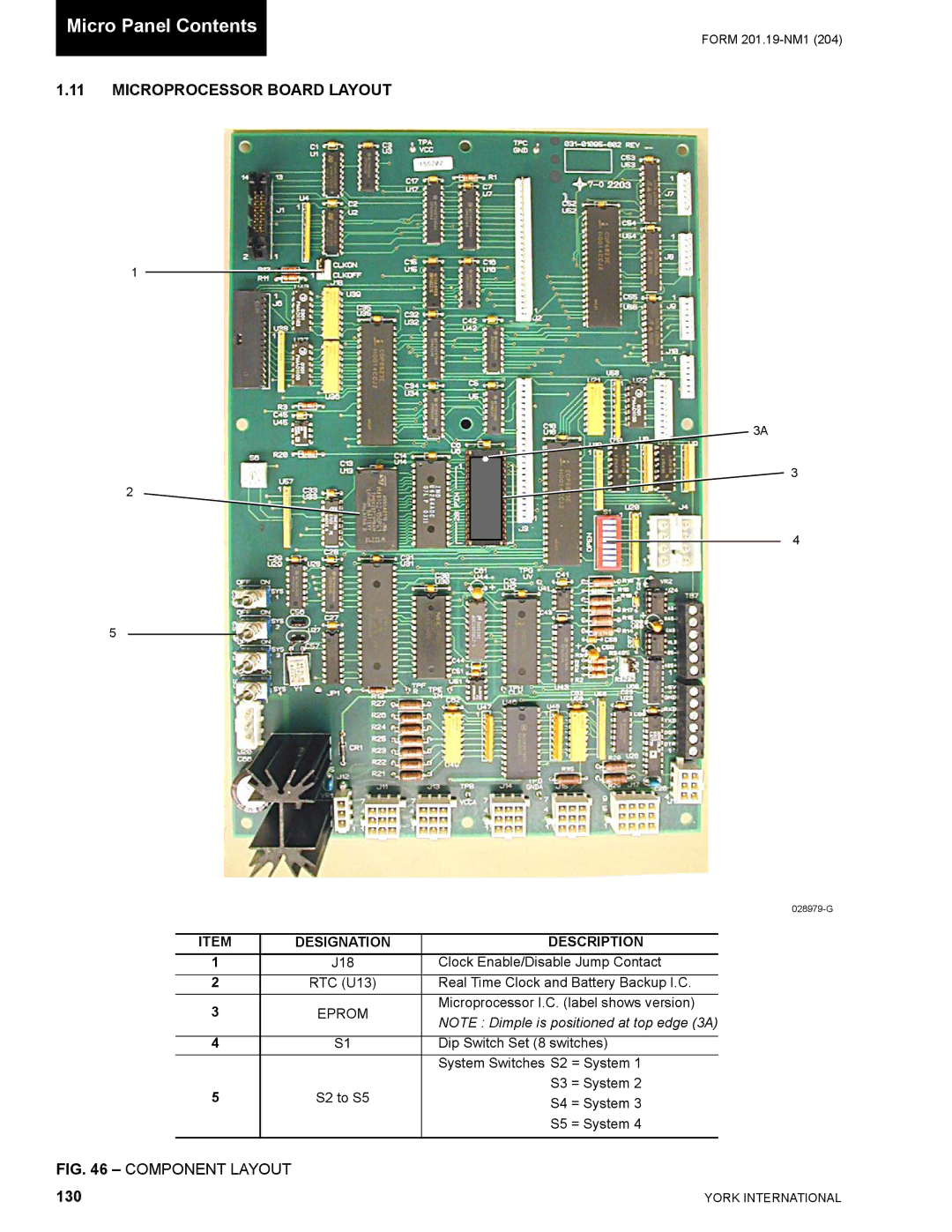
1.11MICROPROCESSOR BOARD LAYOUT
1
2
5
FORM
3A
3
4
ITEM | DESIGNATION | DESCRIPTION |
| ||
1 | J18 | Clock Enable/Disable Jump Contact |
| ||
2 | RTC (U13) | Real Time Clock and Battery Backup I.C. |
| ||
3 | EPROM | Microprocessor I.C. (label shows version) |
| ||
NOTE : Dimple is positioned at top edge (3A) | |||||
|
| ||||
|
|
|
| ||
4 | S1 | Dip Switch Set (8 switches) | |||
|
| System Switches S2 | = System 1 |
| |
5 | S2 to S5 | S3 | = System 2 | ||
S4 | = System 3 | ||||
|
| ||||
|
| S5 | = System 4 | ||
|
|
|
|
| |
FIG. 46 – COMPONENT LAYOUT
130 | YORK INTERNATIONAL |
