Advanced user’s reference manual
HP 50g / 49g+ / 48gII graphing calculator
Page
Printing History
Acknowledgements
Page
Contents
Amort
Names
Algb
Alog
317
COL→
Delalarm
Delay
→COL
359
Expand
Findalarm
EXP2POW
Expan
Iferr
Halt
IBP
IDIV2
List
Not
MAX
Maxr
MIN
Parsurface
PA2B2
Parametric
Parity
3183
Rolld
RND
Rnrm
Roll
3226
TAN
Tabvar
→TAG
Tail
Utpf
Wireframe
Updir
Utpc
Contents
514
→ALG Apeek ARM→ ASM ASM→
610
Vpar
Alrmdat
CST Exited Expr Iopar MASD.INI
Toff Tpar
Understanding Programming
Contents of a Program
Examples of Program Actions
Calculations in a Program
Program Results
To store or name a program
To enter commands and other objects in a program
Entering and Executing Programs
To enter a program
@% @Ér # O4 /3 *!Ì Q3 @Ë@Ï
To stop an executing program
3Q!Ì*4`3/*@Ï
3Q!Ì*4#3/* @Ë@Ï
Program Keys Comments
Level
Osph K
@%SPH% ˜
To switch between entry modes
Viewing and Editing Programs
To view or edit a program
`J!%SPH% @%SPH% ˜
Using Local Variables
Creating Programs on a Computer
Creating Local Variables
`OSPHLV K
Program Comments
Defining the Scope of Local Variables
Evaluating Local Names
Creating UserDefined Functions as Programs
Compiled Local Variables
To include a test in a program
Using Tests and Conditional Structures
Testing Conditions
Key Programmable Description Command
TEST% L
Using Logical Functions
Keys Programmable Description Command
Logical Functions
To enter IFT in a program
Using Conditional Structures and Commands
To enter if then END in a program
Press !%BRCH% !%IF%
Press !%BRCH% L!%IFTE%
To enter if then Else END in a program
Press !%BRCH% @%#IF#%
To enter Ifte in a program or in an algebraic
Conditional Examples
To enter Case END in a program
26 `52 J %TST%
Otst K
Using Definite Loop Structures
Using Loop Structures
While … Repeat … END
Press !%BRCH% !%START%
Start Next Structure
« … start finish Start loopclause Next … »
To enter Start Next in a program
Press ! %BRCH% … %START%
Start Step Structure
« … start finish Start loopclause increment Step … »
To enter Start Step in a program
Press !%BRCH% ! %FOR%
For Next Structure
« … start finish for counter loopclause Next … »
To enter for Next in a program
Press ! %BRCH% … %FOR%
For Step Structure
« … start finish for counter loopclause increment Step … »
To enter for Step in a program
To enter do Until END in a program
Using Indefinite Loop Structures
Do Until END Structure
« … do loopclause Until testclause END … »
Duplicates n, stores the value into n
Press !%BRCH% ! %WHILE%
While Repeat END Structure
« … While testclause Repeat loopclause END … »
To enter While Repeat END in a program
To enter Incr or Decr in a program
Using Loop Counters
Press ! #MEM# %ARITH% %INCR% or %DECR%
∑ j
Using Summations Instead of Loops
To set, clear, or test a flag
Using Flags
Setting, Clearing, and Testing Flags
Types of Flags
Day.month.year format
Recalling and Storing the Flag States
Example
Month/day/year format
To change the current flag states
Using Subroutines
To recall the current flag states
Execute Rclf !L %MODES% %FLAG% L%RCLF%
Torsv K
Torsa K
` 8 J %TORSV%
@·J6 `8 `O%TORSV% !LL%RUN% %DBUG%
To singlestep from the start of a program
To turn off the Halt annunciator at any time
Press !LL %RUN% %KILL%
To singlestep from the middle of a program
To singlestep when the next step is a subroutine
@·J10 `12 O%TORSV% !LL%RUN% %DBUG%
SingleStep Operations
Trapping Errors
Causing and Analyzing Errors
To cause a userdefined error to occur in a program
%ERROR%
To artificially cause a builtin error to occur in a program
To analyze an error in a program
Error Trapping Commands
Iferr then END Structure
Making an Error Trap
« … Iferr trapclause then errorclause END … »
Press !LL %ERROR% !%IFERR%
Iferr then Else END Structure
Press !LL %ERROR% @%IFERR%
To enter Iferr then Else END in a program
Input
Data Input Commands
Using PROMPT, Cont for Input
Key Command Description
@·J %TPROM%
`OTPROMPT ‰
To enter Disp Freeze Halt in a program
Using Disp Freeze HALT, Cont for Input
To respond to Halt while running a program
To respond to Input while running a program
Using INPUT, Enter for Input
« … promptstring commandline Input OBJ→ … »
To enter Input in a program
%VSPH%
Cursorposition
Commandline cursorposition operatingoptions
To design the commandline string for Input
To include Input options
Press @ Õ ! Ê a @
To process the result string from Input
`O Tinput ‰
%TINPU%
To set up an input form
Using Inform and Choose for Input
To set up a choose box
`OPHONES ‰
To enter Wait in a program
Using Wait for Keystroke Input
Beeping to Get Attention
To enter Beep in a program
OUT%
Using KEY for Keystroke Input
Data Output Commands
Output
%TTAG% 1.5 ˜1.85 `
Labeling Output with Tags
Labeling and Displaying Output as Strings
To label a result with a tag
`OTSTRING ‰
Pausing to Display Output
Using Msgbox to Display Output
To set up a message box
Using Menus for Input
Using Menus with Programs
SI%
Using Menus to Run Programs
To create a menubased application
Olst ‰
@·J%EIZ%
To turn off the calculator in a program
Turning Off the Calculator from a Program
%% !Ü.37~@6 68 %%I%% !%%Z%%
@%%I%% 2*%%I%% !%%E%%
Page
FIB1 Fibonacci Numbers, Recursive Version
Fibonacci Numbers
RPL Programming Examples
%FIB1%
FIB2 Fibonacci Numbers, Loop Version
FIB1% !Ü10 N
%FIB2%
FIB2 program listing
10 %FIB2%
Required Programs
Fibt Comparing ProgramExecution Time
Techniques used in Fibt
Structured programming. Fibt calls both FIB1 and FIB2
Techniques used in PAD
Displaying a Binary Integer
PAD Pad with Leading Spaces
13 %FIBT%
Techniques used in Preserve
Preserve Save and Restore Previous Status
PAD program listing
`OPAD K
Preserve program listing
Bdisp Binary Display
`OPRESERVE K
PAD
Techniques used in Bdisp
`OBDISP K
Bdisp program listing
Tile Percentile of a list
Median of Statistics Data
144 %BDISP%
`O%TILE K
Median Median of Statistics Data
Techniques used in %TILE
Tile program listing
Required Program
Techniques used in Median
11 `1 `
Expanding and Collecting Completely
`OMEDIAN K
18 `12 `˜šš
`OMULTI K
Multi Multiple Execution
Techniques used in Multi
Multi program listing
`OEXCO K
Exco Expand and Collect Completely
Techniques used in Exco
Exco program listing
User and system flags for logic control
Minimum and Maximum Array Elements
MNX Minimum or Maximum Element-Version
Ü4 *Y+Z +
`OMNX K
MNX program listing
12 `56 `˜šš 45 `1 `
MNX2 Minimum or Maximum Element-Version
Techniques used in MNX2
MNX2 program listing
Aply program listing
Applying a Program to an Array
%MNX2%
Techniques used in Aply
Make sure the flag 1 is clear to begin
Techniques used in nBASE
Converting Between Number Bases
`OAPLY K
Ô3†2W†4` ‚Å 3 QA *7 `J %APLY% H#DISP ˜˜
NBASE program listing
1000 `23 J %NBASE%
Verifying Program Arguments
`ONAMES K
Names Check List for Exactly Two Names
Techniques used in Names
Names program listing
Techniques used in VFY
VFY Verify Program Argument
VFY program listing
%LIST% %²LIST%
Converting Procedures from Algebraic to RPN
Oben `
Ojeff ` Osarah `
→RPN program listing
Techniques used in →RPN
XQ3 `%²RPN%
Bessel Functions
Techniques used in BER
%BER% !Ü2
BER program listing
`OBER K
%BER%
Sintp program listing
Animation of Successive Taylor’s Polynomials
Sintp Converting a Plot to a Graphics Object
Techniques used in Sintp
`OSETTS K
Setts Superimposing Taylor’s polynomials
Techniques used in Setts
Setts program listing
`OTSA K
TSA Animating Taylor’s Polynomials
Techniques used in TSA
TSA program listing
Temporary menu for data input
Programmatic use of matrices and statistics commands
Programmatic Use of Statistics and Plotting
Techniques used in PIE
Angle
983 %SLICE% 416 %SLICE% 85 %SLICE%
`OPIE K
ßENTER program listing
Trace Mode
Techniques used in αENTER and ßENTER
ΑENTER program listing
`OROOTR K
InverseFunction Solver
Techniques used in Rootr
Rootr program listing
Techniques used in Walk
Animating a Graphical Image
@Å@É x †O3.7
%X²FX% ` 599.5 ` 1 %ROOTR%
`OWALK K
Input/Output
Introduction
Acos
Type
Other Provided Details
How Commands Are Alphabetized
Parallel Processing with Lists
Classification of Operations
Computer Algebra System Commands and Functions
Binary integer
Backup identifier
Realnumber time or angle in hoursminutessecond s format
Library identifier
ABS
Abcuv
ACK
Type Description
Ackall
ASIN, ATAN, COS, Isol
ACOS2S
Symb ACOSHsymb
Acosh
ASIN2C, ASIN2T, ATAN2S
Acosh z
Addtmod
ADD
10z
Addtoreal
Algb
Alog
Principal Interest Balance
Amort
TVM, TVMBEG, TVMEND, Tvmroot
ANS
Animate
Apply
Access …µAPPLY Input/Output
ARC
ARG
Archive
→ARRY
Access …µARRY→ Input/Output
Arit
ARRY→
Access !¼ ¼is the leftshift of the Skey
ASIN2T
ASIN2C
Asinh
ACOSH, ATANH, ISOL, Sinh
ASN
Asinh z
Symb ASINHsymb
Skey
Access … ÃL BIT ASR
ASR
Assume
ADDTOREAL, Unassume
Atan
ACOS, ASIN, ISOL, TAN
ATAN2S
Atan z
Symb ATANsymb
Atanh z
Access …µATICK
Atanh
Atick
#n #m
Access …µATTACH Input/Output
Attach
Augment
BAR
Access …µAUTO Input/Output None
Auto
Axes
Atick xaxis label yaxis label
Access …µAXES Input/Output
AXL
AXM
AXL, AXM, GAUSS, QXA
AXQ
BAR
AXL, AXQ
Baud
Access …µBAR Input/Output None
Barplot
Basis
Bestfit
Access …µBESTFIT Input/Output None
Access … Ã BIN
Beep
BOX
Access !L Pict BOX Is the leftshift of the Nkey
Bins
Blank
#n1 #m1 #n2 #m2 X1, y1 X2, y2
Access …µBUFLEN Input/Output
Buflen
Bytes
C2P
Access … Ã B → R
Cascfg
Case
Cascmd
Help
FLOOR, IP, RND, Trnc
Ceil
Centr
Xunit Nunit Symb CEILsymb
Cholesky
Chinrem
Choose
Command Result
CHR
REPL, SIZE, SUB
Circ
Cksm
NUM, POS
Closeio
Clear
Clkadj
Cllcd
Cmplx
CLΣ
Clusr
Clvar
COL→
→COL
COL
Symb1 Symb2
COL+
Colct
Collect
Symb COMBsymb ,m COMBn, symb COMBsymb ,symb
Colσ
Comb
CON
IDN
Cond
Rarray constant
Carray constant Name
Conic
Access …µCONIC Input/Output None
Conj
Rarray Carray Symb CONJsymb
Conlib
Const
Constants
X1unitssource X2unitstarget X3unitstarget
Cont
Convert
Corr
COV
Access Flags
COS
Cosh
…µCR
Crdir
Cross
Cswp
COL+, COL-, Rswp
Curl
Cyclotomic
Cylin
#n, #m
→PX
Darcy
Date
→date
→DATE
DATE+
Dbug
« program » or program name
Ddays
DEC
Decr
Result See also
Dedicace
DEF
Define
Name=exp Namename Name =expname
Delalarm
DEG
Degree
CR, OLDPRT, PRLCD, PRST, PRSTC, PRVAR, PR1
Delay
RCLALARM, Stoalarm
Delkeys
Xkey1, ... ,xkey n
Access …µDEPND Input/Output
Depnd
Depth
Dervx
Deriv
Desolve
Attach
Access …µDETACH Input/Output
DET
Detach
→DIAG
DIAG→
Diagmap
Diffeq
Diff
DIR
Access …µDIFFEQ Input/Output
Disp
FREEZE, HALT, INPUT, Prompt
Dispxy
Distrib
Obj List
CURL, Hess
DIV
DIV2
DIV2MOD
DIV2
Divis
Divmod
Divpc
END
TAYLOR0, TAYLR, Series
DERIV, DERVX, DESOLVE, ∂
Until testclause END
Doerr
Error
Dolist
SIGNTAB, Tabvar
List List n « program » Results Command Name List n+1
Domain
Dosubs
CNRM, CROSS, DET, Rnrm
List « program » Command Name
DOT
DOLIST, ENDSUB, NSUB, Stream
DRAW3DMATRIX
Access …µDRAW
Access …µDRAX Input/Output None
Draw
Lagrange
Droite
Drop
DROP2
DUP2
Dropn
Dtag
DUP
Dupn
Dupdup
Editb
Edit
Egcd
END
EGV
Egvl
Else
Sign mantissa E sign exponent
Endsub
ENG
EPSX0
Erase
Eqnlib
EQW
EQ→
Euler
ERR0
Errm
Errn
→NUM
Eval
Exlr
Obj See above
EXP
EXP&LN
Ex,y = excosy + iexsiny
EXP2POW
EXP2HYP
Expan
Result X2+X
Expand
Expandmod
COLCT, EXPAND, ISOL, QUAD, Show
Eyept
Expfit
Expln
Expm
…µF0λ
F0λ
Fact
Factor
Factors
Factormod
Modsto
Fanning
Access …µFANNING
FAST3D
FC?
Access …µFAST3D Input/Output None
Access ! Test LL FC ? C
Fcoef
Distrib
Fdistrib
FFT
CF, FC?, FS? FS?C, SF
Finish
Findalarm
Access …µFINISH
Filer
Xunit Nunit Symb FLOORsymb
Flasheval
Floor
FONT6
→FONT
FONT7
FONT8
FONT→
For
Xunit Yunit Symb FPsymb
Fourier
Free
Freeze
CLLCD, DISP, Halt
Froots
FS?
Display Area Value Code
Function
FS?C
CF, FC?, FC?C, FS?C, SF
Fxnd
Access …µFUNCTION
Exlr
AXQ, QXA
Gamma
Gauss
Gbasis
GCDMOD, EGCD, IEGCD, LCM
GCD
Gcdmod
GET
Objget
Geti
GETI, PUT, Puti
#n #m Grob1
GOR
Grad
GET, PUT, Puti
DEG, RAD
Gramschmidt
Graph
Greduce
→GROB
Access …µGRIDMAP Input/Output None
Access …µ→GROB
Gridmap
→LCD, LCD→
Grob
Grobadd
Gxor
GOR, REPL, SUB
Hadamard
Halftan
Halt
Help
Head
HEADER→
→HEADER
CURL, DIV
Hermite
Hess
HEX
Histogram
Hilbert
HMS+
Access …µHISTPLOT Input/Output None
Histplot
HMS
… &9L HMS →
HMS→
→HMS
… & 9L HMS +
Horner
Home
Iabcuv
ABCUV, Iegcd
Ibasis
Ibernoulli
IBP
Chinrem
Ichinrem
IDN
Results See also
Ax+by=c
IDIV2
Iegcd
DIV2, Iquot
Case
Iferr
ELSE, END, IFERR, then
Ifft
∑ Y k e
Obj It depends
IFT
Ifte
Ilap
Rarray Carray Symb IMsymb
Image
LAP, Lapl
…ßIM
Global Global xstart xend
Incr
Indep
Inform
Init
Resets
Title Format Resets Init → vals
Input
INT
Stack prompt Commandline prompt Result
PROMPT, STR→
INTVX, Risch
Integer
Intvx
INV
Invmod
Command INVMOD2 Result
Iquot
Symb1 Global Symb2
Iremainder
Isol
Isom
NEXTPRIME, Prevprime
ISPRIME?
Jordan
Mkisom
BASIS, Image
KER
Kerrm
KEY
Keyeval
Access …µKEYEVAL Input/Output
→KEYTIME
Label
KEYTIME→
Kget
Kill
→LANGUAGE
Access …µ→LANGUAGE Input/Output
Lagrange
LANGUAGE→
Objn Obj1
LAP
Lapl
Last
LCM
Lastarg
LCD→
→LCD
Ldec
Lcxm
HERMITE, Tchebycheff
Lgcd
Libeval
Libs
Title, nlib, nport, ...,title, nlib, nport
Lim
Limit
LIN
Model Form of Expression
Line
Σline
Linfit
→LIST
Linin
Linsolve
LIST→
Πlist
List
Σlist
Access …¹ ¹is the rightshift of the Qkey
Lncollect
Lname
LNP1
Symb LNP1symb
Local
LOG
Ln x +
Logfit
Access !Ø Input/Output
Intercept x Slope x
Access …µLR Input/Output
Full Command and Function Reference 3139
LSQ
Lname
Lvar
MAD
DET, INV
MAP
Access …µMAP Input/Output
Main
Mant
Symb Symb symb
Access …µ↓MATCH Input/Output
Access …µ↑MATCH
↑MATCH
Symb Symb , symb
Maths
Matr
MAX
Input/Output See also
Maxr
Maxσ
Mcalc
BINS, MAXΣ, MINΣ, SDEV, TOT, VAR
Mean
MEM
Menu
RCLMENU, Tmenu
Menuxy
MENU, Tmenu
Merge
MIN
Minehunt
Minr
MINIFONT→
→MINIFONT
Minit
00000000000E-499
Minσ
Mitm
Mkisom
Mod y
MOD
Modsto
Modular
Name Or xunit String
Molwt
Mroot
Msgbox
Msolvr
Mslv
EQNLIB, MCALC, MINIT, MITM, MROOT, MSLV, Muser
Multmod
Muser
→NDISP
NEG
Access …ß NEG ßis the rightshift of the 1key
Ndist
Ndupn
Next
Newob
Nextprime
Noval
Access ! Test L not Is the leftshift of the Nkey
NIP
Not
…µNΣ
Nsub
→NUM
NUM
Numy
Numx
OBJ→
… &NL OBJ →
OCT
OFF
Oldprt
Access …µOPENIO
Access …µOLDPRT
Openio
Global1 ... globaln
Order
Over
Memory Directory Lorder is the leftshift of the Nkey
Xmin, ymin, xmax, ymax, indep, res, axes, ptype, depend
P2C
PA2B2
Parametric
Parity
Access …µPARITY Input/Output
Partfrac
Parsurface
Home directoryname 1 ... directoryname n
Path
Pcar
Pcoef
Pcontour
Access …µPCONTOUR Input/Output None
Pcov
Xmax, ymax
Pdim
Perinfo
Perm
Pick
Pertbl
Peval
Pgdir
Pinit
Pict Command Puts the name Pict on the stack
Pict
Picture
Pixon
Access …µPKT
PIX?
Pixoff
Pmin
Plot
Plotadd
Pmax
An nxn matrix a
Pmini
Polar
Finds the minimal polynomial of a matrix
Form of Current Plotting Action Equation
Access …µPOLAR
Polynomial
POP
Powexpand
Input An expression raised to a power
POS
Potential
PR1
Powmod
Object
Predv
Predx
…µPR1
Preval
Predy
Promptsto
Prevprime
Prlcd
Prompt
Prompt STO
Proot
Propfrac
Global→
Name Name1 name2 Nport global
Prst
Prstc
Prvar
MEAN, PCOV, PVAR, SDEV, TOT, VAR
Psdev
PSI
Psi
Symb String or x or xunit or name
Ptayl
Ptprop
Purge
CLEAR, CLVAR, NEWOB, Pgdir
Push
PUT
Global Global1 ... globaln
Obj put List Name
This command sequence
Puti
Obj put List
Pvars
Pvar
MEAN, PCOV, PSDEV, SDEV, VAR
Pwrfit
Access …µPVARS Input/Output
Nport namebackup Memory
Pview
→Qπ
PX→C
+ c/d*i
LQ, LSQ
Quad
̟ + c/ d* ̟
+ c/ d
Quotient of the Euclidean division
Quot
Quote
Arithmetic, !ÞPOLYNOMIAL !«
Rank
QXA
RAD
Rand
LQ, LSQ, QR
Access …µRATIO
Ranm
Ratio
Steq
Rceq
RCI
Rcij
RCL
Rclalarm
Rclmenu
FINDALARM, Stoalarm
Rclf
Rclkeys
RDM
Rclvx
Rclσ
Rcws
COMB, PERM, Rand
RDZ
…ßL RE
REsymb
Recn
Rect
Recv
New name Old name
Remainder
Rename
Quot
END, While
Reorder
Repeat
Repl
String String result
Plot Type Default Interval
RES
String target
Slopefield
Restore
Backup To restore a
Resultant
Rewrite
Revlist
Risch
Rkferr
RKF
Rkfstep
Problem for a differential equation
Is the rightshift 3key
RNDsymb
RLB
RND
RLB, RR, RRB
Romupload
Rnrm
Roll
Rolld
3207
Root
ROT
ROW
ROW→
ROW+
→ROW
RL, RLB, RRB
Access … ÃL Byte RRB Is the rightshift of the 3key
RPL
RRB
Rref
Rref
RRK
Rrefmod
Rrkstep
− 2 t + t 2
RSD
Rsberr
RKF, RKFERR, RKFSTEP, RRK, Rsberr
DET, IDN
Access … Ã R → B
Rswp
Rules
→Dsymb
Same
→R, IM, RE
180/̟x
Scaleh
Access …µSCALEH Input/Output
Sbrk
Scale
Scatter
Scatrplot
AUTO, SCALEH, Xrng
Sclσ
Access …µSCATTER Input/Output None
Schur
SCI
Send
Sconj
Scroll
Sdev
Series
SEQ
DOSUBS, Stream
Seval
Server
X1/cm3
Show
Sidens
Sigma
Sign
Access !ÖDERIV L
Access !ÖDERIV LL
Sigmavx
ABS, MANT, Xpon
Signtab
SIMP2
SIGNsymb
Sin z
Simplify
SIN
Sincos
Sinh z
Sinh
Sinv
Size
Symb Grob
SLB
Slopefield
String Integer List Vector
Snrm
Sneg
NEG, SCONJ, Sinv
Solveqn
Solve
Solvevx
Solver
Sort
SQsymb
Sphere
Srad
Square Analytic Function Returns the square of the argument
ASR, SL, SLB, SR
SRB
Srecv
COND, SNRM, Trace
SST↓
Access …µSRECV
Srepl
SST
STD
Start
Step
Stime
Access …µSTIME
Step
Steq
Buflen
Stoalarm
Access Input/Output
STO
Óis the rightshift of the 9 key
Access …µSTOF
Stof
Stokeys
Stovx
Store
STO+
STO/, +
DTAG, EQ→, LIST→, OBJ→, →STR
Stoσ
STR→
→STR
List Obj Result
Stream
Strm
Sturm
Sturmab
Sturmab
Stws
SUB
CHR, GOR, GXOR, NUM, POS, REPL, Size
Subst
Subtmod
X1, y1 X2, y2
DIAG→, MIN, SVL
SVD
SVL
Swap
Sylvester
Syseval
SYST2MAT
Symb 1, symb
Tabval
100 y
X, symb
→ARRY
Tabvar
→TAG
Tail
Tan z
TAN
TAN2CS2
TAN2SC
TANHsymb
TAN2SC2
Tanh
Tanh z
HERMITE, Legendre
TAYLOR0
Taylr
Tchebycheff
TDELTAsymb1, symb2
Tcollect
Tdelta
Tests
Then
Teval
Texpand
Text
Tinc
Ticks
Time
→TIME
SIMPLIFY, TCOLLECT, Texpand
Tlin
Tline
TINCsymb1, symb2
Tran
Tmenu
TOT
Trace
BAUD, CKSM, Parity
Transio
Trig
Effect
Trigtan
Trigcos
Trigo
Trigsin
Trnc
TRN
CONJ, Tran
TRNCsymb
Trunc
Truth
TRNCz
Tsimp
Access …µTRUTH Input/Output None
Tstr
Tvmend
Tvars
TVM
Tvmbeg
Object Type Number User objects
Builtin Commands
Type
Ubase
Unassume
Ufact
UFL1→MINIF
Unassign
→UNIT
Unbind
Unpick
Utpc
Unrot
Until
Updir
UTPC, UTPN, Utpt
Utpf
Utpn
UTPF, UTPN, Utpt
Uval
Utpt
UVALsymb
X1, x2, ..., xn Xn-2
Flag -16 clear Rectangular mode Flag -16 set Polar mode € y
Coordinate System -16, Complex Mode
X1, x2
VAR
Vandermonde
Version
Access …µVERSION Input/Output
Vars
VER
Visitb
Variable name Contents opened in the command line Editor
Variable name Contents opened in the most suitable Editor
Visit
Vtype
Access ! L in Wait Is the leftshift of the Nkey
Wait
While Repeat
Wireframe
While
While testclause Repeat loopclause END
Wslog
Log4 ... log1
Access …µWSLOG
Access …µΣX Input/Output
ΣX2
Xmit
ΣX2
Xcol
Xget
Xnum
Access …µXMIT
XOR
MANT, Sign
Xpon
Xput
XPONsymb
Xrng
Command XQ.3658 Results 1829/5000
Command XQ.3658 Results √19/142
Xrecv
Input/Output RPN
Access …µXSEND
Xsend
Xserv
ΣX*Y
Xvol
Xxrng
ΣXY
…µΣY
ΣY2
ΣY2
Ycol
Yslice
Yrng
AUTO, PDIM, PMAX, PMIN, Xrng
EYEPT, XVOL, XXRNG, YYRNG, Zvol
Yvol
Yyrng
Zeros
Zvol
Power
Access Q
Zfactor
Symbz
Where
√ Square Root
Zsymb
SQ, , Isol
Lower limit, upper limit, integrand, name
Access …Á Áis the rightshift of the Ukey
Integrate
? Undefined
Results -π/2
∞ Infinity
Summation
Sigma Plus
X 2, …, x m 1, …, x 1 m x n 1, … , x n m
Access …µΣ+ Input/Output
Access …µΣ Input/Output
Sigma Minus
Symb Name Xunit
∂ Derivative
Factorial
14159265359…
Symb,x
Percent
Unit attachment
Xy/100
Less than
« » Program delimiters
Type Object Description
#n1 #n2
≤ Less than or Equal
≥ Greater than or Equal
Greater than
≠ Not equal
≠ symb
Multiply
+ Add
Subtract
Divide
Y1/unit
= Equal
== Logical Equality
… É
Store
→ Create Local
DEFINE, RCL, →, STO
CLEAR, DROP, DROPN, DROP2
Semicolon
CAS directory, Casdir
CAS Settings
Selecting CAS Settings
Points to note when choosing settings
Computer Algebra System
Extending the CAS
Using the CAS
Examples and Help
Compatibility with Other Calculators
Arithmetic Integer commands, !ÞINTEGER
Computer algebra command categories listed by menu
Arithmetic commands
Algebra commands, …×
Arithmetic Permutation commands, !Þ Permutation
Arithmetic Modulo commands, !Þ Modulo
Other Arithmetic commands, !Þ
Calculus commands
Operations, !Ø Operations
Exp and Lin commands, !Ð
Matrixrelated commands
Create, !Ø Create
Eigenvectors, !Ø Eigenvectors
Quadratic form, !Ø Quadratic Form
Linear Systems, !Ø Linear Systems
Linear Applications, !Ø Linear Appl
Hyperbolic, …Ñ Hyperbolic
Symbolic solve commands, !Î
Trigonometry commands
Other Trigonometry commands, …Ñ
Trigonometric conversions, !Ú Trig Conv
Convert commands, !Ú
Unit conversion tools, !Ú Units Tools
Base conversion tools, !Ú Base
Matrix convert, !Ú Matrix Convert
Other CAS operations, …µ
These commands display menus or lists of CAS operations
CAS menu commands, …µ
CAS utility operations
Equation Reference
Equation Reference
FLUIDS, 24 *********************3
Internal bending moment at
Columns and Beams
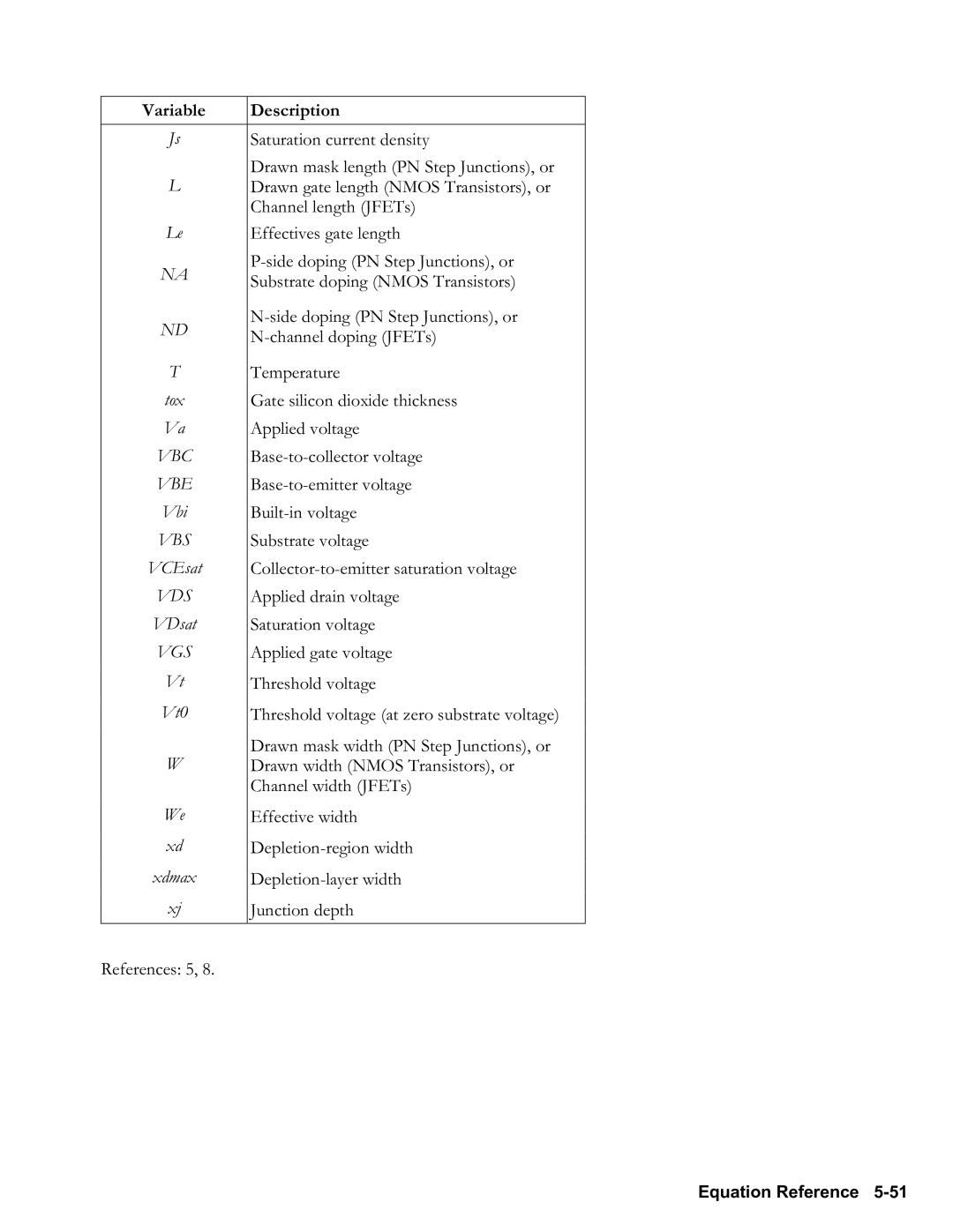
Variable Description
Σcr Critical stress Σmax Maximum stress
Example
Elastic Buckling 1
Eccentric Columns 1
Equations
Simple Slope 1
Simple Deflection 1
Equation
Simple Moment 1
Solution V=624.387lbf
Simple Shear 1
Cantilever Slope 1
Cantilever Deflection 1
Cantilever Moment 1
Cantilever Shear 1
Solution V=200lbf Equation Reference
Relative permittivity
Electricity
Relative permeability
Coulomb’s Law 2
Ohm’s Law and Power 2
Voltage Divider 2
Wire Resistance 2
Solution V1=80V
Solution I1=5.6250A
Series and Parallel R 2
Solution R=0.175
Series and Parallel C 2
Inductive Energy 2
Solution V=50V
Series and Parallel L 2
Capacitive Energy 2
Capacitor Charge 2
RLC Current Delay 2
Solution q=0.0020C Equation Reference
DC Capacitor Current 2
RL Transient 2
Solution V=3.2968V
DC Inductor Voltage 2
RC Transient 2
Cylindrical Capacitor 2,19
Solution I=0.0072A
Resonant Frequency 2
Plate Capacitor 2
Toroid Inductance 2
Solenoid Inductance 2
Sinusoidal Voltage 2
Fluids
Sinusoidal Current 2
Initial and final velocities
Pressure at Depth 3
Bernoulli Equation 3
Reynolds number
Flow with Losses 3
Flow in Full Pipes 3
Forces and Energy
Linear Mechanics 4
Centripetal Force 4
Angular Mechanics 4
Hooke’s Law 4
MassEnergy Relation 4
1D Elastic Collisions 4
Drag Force 4
Law of Gravitation 4
Ideal Gas Law 5
Gases
Polytropic Processes 5
Solution Vf=21
Ideal Gas State Change 5
Isothermal Expansion 5
Real Gas State Change 5
Real Gas Law 5
Kinetic Theory 5
Heat Transfer
Thermal Expansion 6
Heat Capacity 6
Conduction 6
Conduction + Convection 6
Convection 6
Ia, Ib
Magnetism
Black Body Radiation 6
Fba
Force between Wires 7
Straight Wire 7
Magnetic B Field in Solenoid 7
Solution B=0.0785T
Magnetic B Field in Toroid 7
Motion
Object in Free Fall 8
Linear Motion 8
Projectile Motion 8
Escape Velocity 8
Angular Motion 8
Circular Motion 8
Terminal Velocity 8
Law of Refraction 9
Optics
Brewster’s Law 9
Critical Angle 9
Thin Lens 9
Solution n2=1.5000
Spherical Reflection 9
Spherical Refraction 9
Oscillations
Simple Pendulum 10
MassSpring System 10
Example Given L=15cm
Torsional Pendulum 10
Conical Pendulum 10
Simple Harmonic 10
Plane Geometry
Ellipse 11
Circle 11
Equations Example
Regular Polygon 11
Rectangle 11
Triangle 11
Circular Ring 11
Cone 12
Solid Geometry
Parallelepiped 12
Cylinder 12
Sphere 12
Solid State Devices
Channel length JFETs
Saturation current density
Drawn mask length PN Step Junctions, or
Drawn gate length Nmos Transistors, or
PN Step Junctions 13
VDS
Nmos Transistors 13
JFETs 13
Bipolar Transistors 13
Xdmax = ⋅ Vbi VGS + VDS
Maximum principal normal stress
Stress Analysis
Minimum principal normal stress
Shear Stress 14
Normal Stress 14
Stress on an Element 14
Example
Mohr’s Circle 14
Transverse Waves 15,1
Waves
Longitudinal Waves 15
Sound Waves 15
References
Page
Development Library
Development Library
Development Library Command Reference
Obj String
Obj1 … objn Symb Obj1, ...,objn
Code String
BetaTesting
String Obj Debug string Error list
String Obj
Library Object String
String Error list Edited string
Library n
Ey,z.Et
LC~C
Obj … obj Obj 1, ...,obj n
→LST
Obj 1 … obj n Obj 1, ...,obj n
Pokearm
String Global
→S2
String1 String2
Returns
Xlib
Crlib Create Library Command
Extension program
Modes
Masd The Machine Language and System RPL Compiler
Introduction
Starting Masd
Format of the error list
Errors
Error messages Message Description
Labels
Links
Constants
Extable
Expressions
Macros and includes
Operator Priority
Compilation directive
Filename conventions
Directive Description
Docstr
!DBGINF directive
CPU architecture
Saturn ASM mode
Bit registers
New instructions
Other notes
Skips
These instructions Are equivalent to
Skips instructions Equivalents
Tests
Syntax Example
Saturn instructions syntax
Syntax Example
DReg=hh
See above. This is only valid in emulated Saturn
Places the value of Exp in the code, on x nibbles
CARRY0
003AA Autousertest
ARM architecture
ARM mode
Description Form
Instruction set
Operation Assembler Action Flags
REG B
Armsat instruction
Offset Element
REG a
REG C REG D REG R0 REG R1 REG R2 REG R3 REG R4
Unnamed local variables
System RPL mode
Instructions
Reals and system binary
Tokens
Defines
Token Description
Code
LC 001 Gosbvl Outcinrtn ?CBIT=1.6
Turnmenuoff
LC 80100 Armsat
Level
Disassemblers
String String 1, ...,string n
Entry Point Library Extable
Library
Nop
C0C
Error and Status Messages A1
Messages Listed Alphabetically
Message Meaning # hex
A2 Error and Status Messages
Error and Status Messages A3
Σdat
A4 Error and Status Messages
Error and Status Messages A5
A6 Error and Status Messages
C0D
Error and Status Messages A7
C0E
C0B
A8 Error and Status Messages
# hex Message General Messages
Error and Status Messages A9
# hex Message
A10 Error and Status Messages
OutofMemory Prompts
Error and Status Messages A11
Equation Writer Application Messages
Stack Errors and Messages
A12 Error and Status Messages
Object Editing Messages
Statistics Messages
# hex Message FloatingPoint Errors
Error and Status Messages A13
Array Messages
A14 Error and Status Messages
Mode and Plot Input Form Prompts
# hex Message 70F
Error and Status Messages A15
73F
A16 Error and Status Messages
75F
Error and Status Messages A17
78F
A18 Error and Status Messages
Error and Status Messages A19
Advanced Statistics Messages
A20 Error and Status Messages
80F
Error and Status Messages A21
82F
A22 Error and Status Messages
85F
Error and Status Messages A23
87F
A24 Error and Status Messages
Statistics Help Messages
Error and Status Messages A25
HP Solve Application Messages
Programmer’s Doerr
# hex Message Unit Management
Printing
Time Messages
Error and Status Messages A27
System Flags Choose Box Prompts
A28 Error and Status Messages
Error and Status Messages A29
A30 Error and Status Messages
Error and Status Messages A31
Prompts
A32 Error and Status Messages
Error and Status Messages A33
A34 Error and Status Messages
Statistics Prompts
Error and Status Messages A35
A36 Error and Status Messages
Time and Alarm Prompts
Error and Status Messages A37
A38 Error and Status Messages
Symbolic Application Prompts
Plot Application Prompts
Error and Status Messages A39
A40 Error and Status Messages
Error and Status Messages A41
Solve Application Prompts
A42 Error and Status Messages
Error and Status Messages A43
A44 Error and Status Messages
CAS Messages
Error and Status Messages A45
A46 Error and Status Messages
Error and Status Messages A47
DF1A DF1B DF1C DF1D DF1E DF1F
A48 Error and Status Messages
Filer Application Messages
DF0A DF0B DF0C DF0D DF0E DF0F
Constants Library Messages
Error and Status Messages A49
MultipleEquation Solver Messages
A50 Error and Status Messages
Equation Library Messages
Minehunt Game Prompts
Development Library and Miscellaneous Messages
Error and Status Messages A51
Periodic Table Messages
Financial Solver Messages
A52 Error and Status Messages
Tables of Units and Constants B1
Units
B2 Tables of Units and Constants
Tables of Units and Constants B3
B4 Tables of Units and Constants
Constant Full Name Value in SI Units
Tables of Units and Constants B5
B6 Tables of Units and Constants
Properties of Elements
System Flags C1
System Flags
Flag Description
Not used
C2 System Flags
System Flags C3
C4 System Flags
System Flags C5
C6 System Flags
System Flags C7
C8 System Flags
Internal use only /0 occurred
System Flags C9
User Flags
Page
Reserved Variables D1
Contents of the System Reserved Variables
Reserved Variables D3
ΒENTER
D4 Reserved Variables
Exited
Reserved Variables D5
Nmines
MHpar
Mpar
N1, n2
Reserved Variables D7
BAR, etc
D8 Reserved Variables
Prtpar
Reserved Variables D9
S1, s2
D10 Reserved Variables
Parameter Description Default Value Command
To use for input into the table
NUMX, Numy
Statistical Matrix for Variables 1 to m
Var1 var2 … varm
Reserved Variables D11
D12 Reserved Variables
EXPFIT, PWRFIT, or Logfit
Casdir Reserved Variables
D14 Reserved Variables
Modulo
Object Type Size bytes
Object Size
Technical Reference E1
Pattern Antiderivative
Symbolic Integration
E2 Technical Reference
Technical Reference E3
E4 Technical Reference
→DEF Expansions
Technical Reference E5
Order Operation
E6 Technical Reference
International Standard publication No. ISO 31/l197 8 E
Parallel Processing with Lists F1
Group 1 Commands that cannot parallel process
Group 2 Commands that must use Dolist to parallel process
General rules for parallel processing
F2 Parallel Processing with Lists
Group 5 Commands that set modes / states
Group 6 Oneargument, oneresult commands
Group 4 ADD and +
Group 10 Quirky commands
Group 7 Two argument, one result commands
Group 8 Multipleargument, oneresult commands
Group 9 Multipleresult commands
F4 Parallel Processing with Lists
Using Dolist for Parallel Processing
$ & +
$ & C
$ & D
$ & F
~@ & O
Keycode Keystroke Definition
¥ ! &I
@ & ³ @ & O
@%VARNAME% = varname
~@ & Í @ &†
Keyboard Shortcuts G3
G4 Keyboard Shortcuts
Syntax Example
Menu Numbers
MenuNumber Table H1
H2 The MenuNumber Table
Menus 0 through
MenuNumber Table H3
H4 The MenuNumber Table
Menus 118 through
BuiltIn Library Menus
Menus 178 through
MenuNumber Table H5
Page
Key ALPHARS2 MTH NXT Prob
Command MenuPath Table
+ key
I2 The Command MenuPath Table
Command Type Library Size Keys Menu First
CAT Algb
MTH List
Arith Modul
«MODULAR» Addtoreal
I4 The Command MenuPath Table
CHR
LS&MODE Flag
PRG Test NXT NXT PRG NXT Modes Flag Chinrem
PRG NXT
I6 The Command MenuPath Table
PRG NXT NXT Time NXT
CAT Delalarm
PRG NXT NXT Time Alrm Delay
RS&TIME NXT
I8 The Command MenuPath Table
Else
PRG NXT NXT Error Iferr
«POLYNOMIAL» EGV
MTH Matrx NXT
I10 The Command MenuPath Table
I11
I12 The Command MenuPath Table
«DIFF» NXT NXT
Calc Deriv NXT
«INTEGER»
PRG Brch NXT
I14 The Command MenuPath Table
I15
I16 The Command MenuPath Table
I17
I18 The Command MenuPath Table
I19
I20 The Command MenuPath Table
I21
I22 The Command MenuPath Table
I23
I24 The Command MenuPath Table
I25
I26 The Command MenuPath Table
I27
I28 The Command MenuPath Table
XLIB~
Matrices Creat NXT NXT MTH Matrx Make NXT NXT
DUP Menuxy Version
CAT Vtype
MTH NXT Const «CONSTANTS»
I30 The Command MenuPath Table
SLV NXT
Alphalse
→ALG
Σline
Σlist
PRG Test «TESTS» NXT
I32 The Command MenuPath Table
Character Codes
Code Description
Ascii Character Codes and Translations J1
J2 Ascii Character Codes and Translations
Code Trans. Description
Index
Alpha keyboard
Calculator
59, 531
375 Preserving calculator status
Flags
132
Last argument
Memory
Nested structures
545
Programs
Range 3115
Serial communications
237, D3
Tagged objects
UPs