HP Part No Microfiche Part No Edition
User’s Handbook
Restricted Rights
Certification Warranty
Assistance Safety Notes
If this instrument is used in a manner not specified by
General Safety Considerations
Before switching on this instrument, make sure that the line
Vii
Figure O-l. Typical Serial Number Label
Typeface Conventions
Manufacturer’s Declaration
Regulatory Information
Declaration of Conformity
Manufacturer’s Address
Declaration of Conformity
Xii
Instrument MarkingsA
US Field Operations
Hewlett-Packard Sales and Service Offices
Contents
HP-IB
Contents-2 User’s Handbook
Contents-3
Contents-4 User’s
Delta Ma&e+
Contents-6
Freq Mult Freq Offset
Contents-6 User’s
Local
Marker
Contents-8 User’s
Recall
Contents-9
User Defined Menu
Contents-l User’s
ZeroFreq
AM,FM
Contents-13
Contents-14 User’s
Figures
Contents-15
ALC
Contents-16
Tables
Getting Started Introduction l-1
What Is In This Chapter
Equipment Used In Examples
How To Use This Chapter
Getting Started Introduction
Getting Started Basic
Introducing HP 8360 Series Synthesized Sweepers
Getting Started Basic l-3
Figure l-2. Display
Display Area
Getting Started Basic l-5
Entry Area
CW Operation
CW Operation Start/Stop Frequency Sweep
Start/Stop Frequency Sweep
CW Operation and Start/Stop Frequency Sweep
Center Frequency/Span Operation
Getting Started Basic l-9
Center Frequency and Span Operation
Power Level Operation
Power Level Sweep Time Operation
Getting Started Basic l-l
Power Level and Sweep Time Operation
Continuous, Single Manual Sweep Operation
Continuous, Single, and Manual Sweep Operation
Marker Operation
Marker Operation
Saving Recalling an Instrument State
Getting Started Basic l-17
Saving and Recalling an Instrument State
Power Sweep Operation
Power Sweep Power Slope Operation
Getting Started Basic l-19
Figure l-10. Power Sweep and Power Slope Operation
Table l-l. Keys Under Discussion in This Section
Advanced
Getting Started Advanced
Advanced Table l-l Keys Under Discussion in This Section
Externally Leveling the Synthesizer
Hint
12 shows the input power versus output voltage
60 dBV
10 mV Detector Input POWER, dBm
External Leveling Used With the Optional Step Attenuator
Getting Started Advanced l-27
Leveling with Power Meters
Leveling with MM-wave Source Modules
Awplifier
Working with Mixers/Reverse Power Effects
Ig-y-LO Ll%EL
SwrNEsl2ER WlTN OPflON Do1
= +lO dBm
5dBm Measures -8 dBm
Working with Spectrum Analyzers/Reverse Power Effects
Creating and Applying User Flatness Correction Array
Optimizing Synthesizer Performance
Creating a User Flatness Array Automatically, Example
Getting Started Advanced l-35
Select Auto Fill Stop a@=, Auto Fill Incr aGHz
Creating a User Flatness Array, Example
19. Creating a User Flatness Array
Activate List Mode
Example
Synthesizer
Band power sensors are not available from
Enable User Flatness Correction
Figure l-2 1. Scalar System Configuration
On the synthesizer, press Power Cm. Select
Getting Started Advanced l-45
Getting Started Advanced
Using Detector Calibration
Getting Started Advanced
Tracking
Peaking
ALC Bandwidth Selection
Select Step Swp Menu
Using Step Sweep
Creating and Using a Frequency List
Getting Started Advanced l-53
Using the Security Features
User Defined Preset Recalled
Changing the Preset Parameters
Getting Started Programming l-55
Programming
HP-IB General Information
Interconnecting Cables
Programming the Synthesizer
Halt Reset
HP-IB Command Statements
Abort
ABORT7
Remote
Remote
Resume
Local Lockout
Clear
Local
CLEAR7
Getting Started Programming l-59
Output
Reset Control Send
Convert Image Iobuffer Transfer
ENTER719USING
Enter
Convert Image Iobuffer On Timeout SET Timeout Transfer
Query
Getting Started with
Command Examples
Command Mnemonics
Angle Brackets
Response Examples
Forgiving Listening and Precise Talking
Program and Response Messages
Page
Paths Through the Command Tree
Figure l-25. a Simplified Command Tree
Semicolon
Aabbff Aabbgg
Figure l-26. Proper Use of the Colon and Semicolon
Reading the Command Table Getting Started Programming
Subsystem Command Tables
Auto
State Power Level
More About Commands
Program Message Examples
Parameter Types
MAX
Repeat
Reading Instrument Errors
Print
Example Program
Output OStimulus*IDN? Enter OStimulusId$ Print Id$
Getting Started Programming
This Subsection
Details Commands Responses
Program Message Syntax
Getting Started Programming l-79
Common Command Syntax
Subsystem Command Syntax
Getting Started Programming l-81
Response Message Syntax
Scpi Data Types
Discrete
Examples of numeric Parameters 100
Response Data Types
Getting Started Programming l-85
SO is this
Programming Typical Measurements
Using the Example Programs
Sample Synthesizer Commands
Use of the Command Tables
HP-IB Chec Example lrogram
Command Parameters Parameter Type Allowed Values POWer
Program Comments
Local Lockout Demonstration Example Program
Pause
Local Lockout Print
Hint
Setting Up a Typical Sweep, Example Program
Program Comments
Queries, Example Program
Getting Started Programming l-93
Saving and Recalling States, Example Program
Pause
Looping Synchronization Example Program
Using the *WAI Command, Example Program
Program Comments
Clear Screen
Using the User Flatness Correction Commands Example Program
Subend
END While
Fnend
Getting Started Programming l-101
Condition Register
Transition Filter
Enable Register
Event Register
An Example Sequence
Case a Case B Case C Case D Condition N-L TlT2T3T4T5
04 Getting Started Programming
Overview
Getting Started Programming l-1
Figure l-36. Inside the Idle State
Getting Started Programming l-107
Page
Init Configuration
Common Trigger Configurations
Getting Started Programming l-109
10 Getting Started Programming
Trig Configuration
Getting Started Programming l-l11
Description Triggering in the HP Series Synthesizers
Trigger Keyword Definitions
Advanced Trigger Configurations
BUS
12 Getting Started Programming
IMMediate
ODELay
SOURce
HP Basic
USA
Related Documents
14 Getting Started Programming
Operating and Programming Reference
Operating and Programming Reference
Function Group Menu Map Description
Address
Programming Codes See Also
Function Group System Menu Map
Scpi NONE, see the individual softkeys listed
Function Group ALC Menu Map
ALC System Overview
Page
Operating and Programming Reference User’s
Operating and Programming Reference A-7
Figure A-2. Typical External Leveling Hookup
Operating and Programming Reference A-9
See Also ALC, ALC BW Menu
ALC Bandwidth Select Auto
ALC Bandwidth Select Low
Programming Codes Scpi
See Also ALC
See Also RECALL,SAVE
Function Group Menu Map Description Programming Codes
Function Group User CAL Menu Map
AM BW Cal Once
Function Group MOD Menu Map
AM Menu
MOD Modulation
AM On/OffIO dBfV
Function Group Ilvloo Menu Map
AM On/Off Ext
Function Group Marker Menu Map
AM On/Off In-t
AM Type 10 dB/V
LALC, CONNECTORS, Iniod
None
Programming Codes
RQS
Arrow Keys
Arrow Keys
Scpi Status Register
Entry None
User Defined None
EiEi
TOO Many Correction PTS Requested
Menu Map 2,s
TOO Many List PTS Requested
Auto Fill #Fts
Auto Fill Start
Programming Codes Scpi CALibrationTRACk
Function Group POWER, User CAL Menu Map 5,9
Blank Disp
Frequency None
See Also SPAN,m,STOP
Service
See Also Fault Menu
See Also w
SHMZ18HZ Shkzohz
# of Times to Clear Memory
Function Group P O W E R Menu Map
BNC Connectors
Programming Codes Scpi NONE, see Fltness Menu
Operating and Programming Reference C-5
Connectors
Figure C-l. Auxiliary Interface Connector
Table C-l. Pin Description of the Auxiliary Interface
Out
Operating and Programming Reference C-9
MTA
Operating and Programming Reference C-l
Figure C-3. Interface Signals of the Source Module Connector
Sweep
Copy List
CorPair Disable
W E R
See Also Aalc
Coupling Factor
Frequency
$iEqICW
CW/CF Coupled
Programming Codes Scpi None
Dblr Amp Menu
Deep AM
Delay Menu
Function Group Modulation Menu Map
Ammode Deep
Delete All
Delete Menu
Menu Map 2,5
Menu Map ‘4
Delete Current
Delta Marker
Delete Undef
Disp Status
Delta Mkr Ref
Function Group System Menu Map k
Marker
Table D-l. Mnemonics used to Indicate Status
Disp Status
Function Group Power Menu Map
Daubler Amp Mode Auto
Table D-l Mnemonics used to Indicate Status
See Also Dblr hnp Menu
Doubler Amp Mode Off
Function Group Frequency Menu Map
Dwell Coupled
Enter Corr
Adrs
System
Enter List Dwell
Enter Freq
Programming Codes Scpi NONE, see Fitness Menu
Programming Codes SCPINONE, see Fltness Menu
Description Programming Codes See Also
Enter List Freq
Programming Codes Scpi NONE, see List Menu
See Also List Menu
Enter List Offset
Entry Keys
Ext Det Cal
Function Group Service Menu Map
Fault Menu
Operating and Programming Reference User’s
Programming Codes SCPISee Fault Menu
Fault Info
Pwron Fail
Calco Fail
TMR
Calyo Fail
Cnflct
Fail Search
Fltness lbnu
Fitness Menu
Start stop # Pts Correction Undefined More Incr
Frequency MHZ 10 1 1 0 0 0 0 0 0 2 1 0 0 0 0 0
Theory of operation
Operating and Programming Reference F-9
Fitness EIenu
FM Coupling 1OOkHz
FM Coupling DC
FM adaff
FM Menu
FM On/Off AC
MOD, Connectors
FM On/Off DC
Modulation
Function Group &j@ Menu Map
See Also MOD,CONNECTORS EN On/Off Ext
Freq Cal Menu
FM On/Off Int
Function Group IhnoD Menu Map
Frequency Menu
Freq Follow
Operating ahd Programming Reference
Freq Mult
Freq Offset
Freq Offset
FulliTsr Cal
Global Offset
Global Dwell
HP-IB Menu
HP-IB Address
Ciil
See Also CONNECTORS, HP-IB Getting Started Programming
Unitam Dbpct
Internal AM Depth
Internal AM Waveform Noise
Internal AM Rate
Internal AM Waveform Sine
Internal AM Waveform Ramp
Internal AM Waveform Triangle
Internal AM Waveform Square
Internal FM Rate
Internal FM Deviation
Ramp
Noise
Function Group
Menu Map Description
Internal FM Waveform Square
Internal FM Waveform Sine
Internal Menu
Internal FM Waveform Triangle
Function Group Iniod Menu Map
Internal Pulse Generator Period
Internal Pulse Generator Width
Internal Pulse Generator Rate
Function Group Imod Menu Map
Function Group IlvloD Menu Map
Internal Pulse Mode Gate
Internal Pulse Mode Auto
Function Group MOq Menu Map
Invert Input
Internal Pulse Mode Trigger
Leveling Mode ALCof f
Leveling Mode Search
Leveling Mode Normal
Leveling Point Intrnl
Leveling Point ExtDet
Leveling Point Module
ALC, Connectors
Leveling Point PwrMtr
Programming Codes See Also
List Menu
Global Duel1
Operating and Programming Reference L-7
List Mode Pt Trig Bus
List Mode Pt Trig Auto
Instrument State None
List Mode Pt Trig Ext
Manual Sweep
Ml--M2 Sweep
Function Group Sweep Menu Map
KimaL Suesp
Amp1 Markers Center=Marker
Function Group Menu Select Menu Map
Marker Ml
Marker M3
Marker M2
Marker M5
Marker M4
See Also
Measure Corr All
Markers All Off
Programming Codes Scpi MARKerAOFF
Measure Corr Undef
Measure Corr Current
Meter On/Off AM
Meter Adrs
Programming Codes Scpi MEASureFM?
Meter On/Off FM
ModOut On/Off AM
ModOut On/Off FM
Modulation
Figure M-l. ALC Block Diagram
Amplitude Modulation
Operating and Programming Reference M-15
User’s Handbook Amplitude Modulation
Figure M-2. Power Accuracy Over the AM Dynamic Range
User’s Handbook FM Modulation
FM Modulation
Operating and Programming Reference M-17
Figure M-3. FM Deviation and Rate Limits
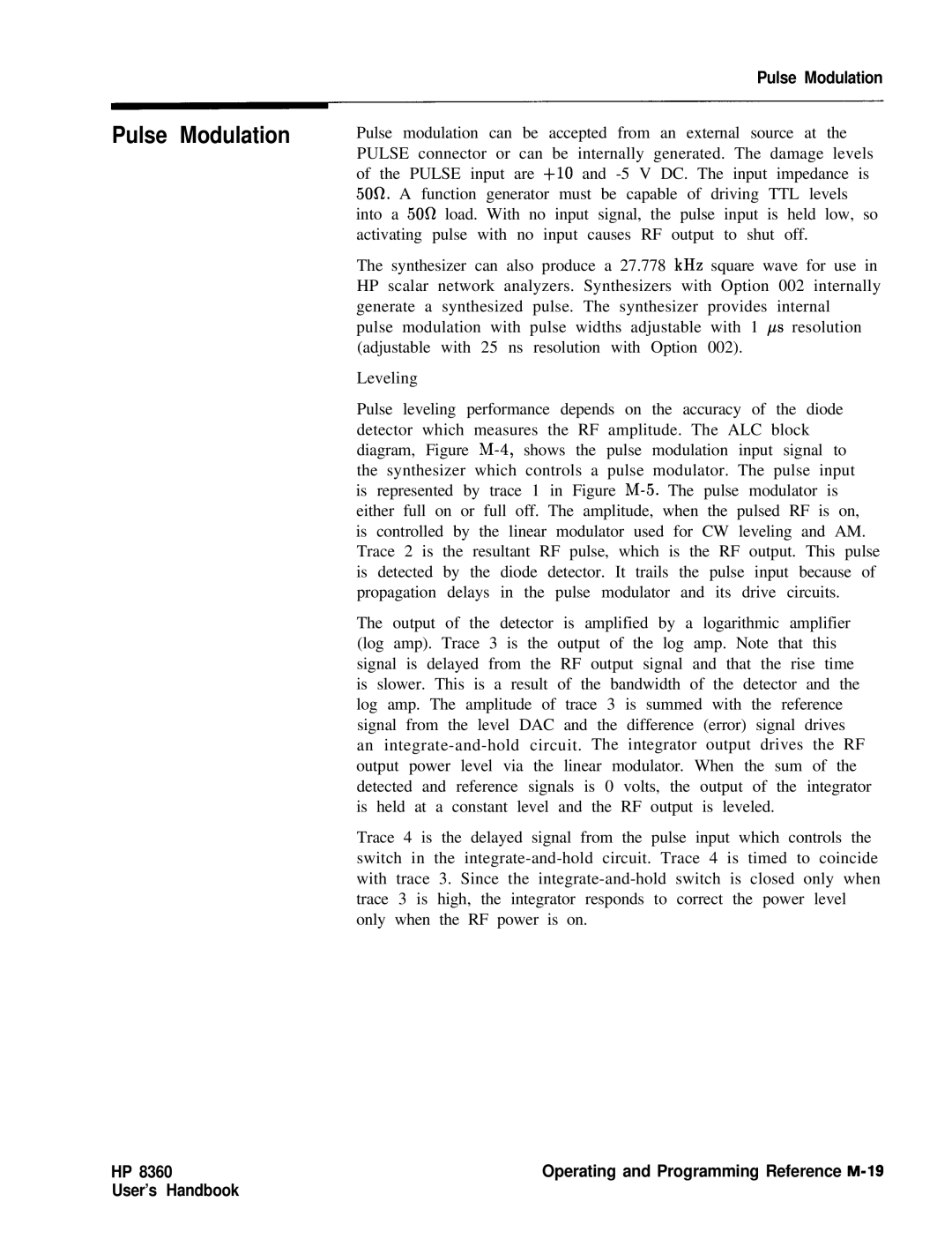
Pulse Modulation
Pulse Modulation
Figure M-4. ALC Block Diagram
Operating and Programming Reference M-21
Figure M-8. Video Feedthrough
Module Menu
Module Select Auto
Module Select Front
Module Select None
Mudule Select Rear
Monitor Menu
ALL Function Groups ALL Menu Maps
More n/m
Mtr Meas Menu
Peak RF Always
Peak RF Once
Power None
INT
PowerdBm INT
See Also ALC, CONNECTORS, Det Gal Menu, Fltness ON/OFF
Power iZiG
Power Slope
Power Offset
Power Sweep
Scpi SYSTemPRESetEXECute
Preset Mode Factory
Printer Adrs
Preset Mode User
Figure P-l. How Prior Works
Menu Select None
Programming Language Ciil
Programming Language Scpi
Pt Trig Penn
Pulse Delay Normal
Function Group Menu Map Description IhnoD1
Pulse Delay Trigd
Function Group MOD
Pulse Menu
Pulse an/Off Ext
Pulse On/Off Intrnl
Pulse h/Off Extrnl
MOD
Pulse On/Off Scalar
Pulse Rate
Pulse Period
Pulse Rise Time Fast
Pulse Rise Time klto
Pulse Width
Pulse Rise Time SlQW
Function Group Ialc Menu Map
Pwr Mtr Range
Ref Osc Menu
Rotary Knob
Programming Codes Scpi *SAV num
Save Lock
Save User Preset
User’s Handbook Scpi Conformance Information
Mode MODE? Span
Auto AUTO?
Operating and Programming Reference S-3
SPAN?
Mode MODE?
Stop STOP?
Aoff
Operating and Programming Reference S-5
Step STEP? Time Auto AUTO?
Gpib
TIME?
Abus
ABUS?
Operating and Programming Reference S-7
TINT?
Mode MODE? Type TYPE?
A4VCO
Agvco
Save Zero ALL
Zero Type
Code
Span Auto AUTO?
List
Step Auto AUTO?
Msib
Slew SLEW? Auto AUTO?
Xfer
Save Type
KEY
Introduction
Ieee 488.2 Common Commands
Scpi Command Summary
Listmodeauto
Operating and Programming Reference S-17
Scpi Command Summary
Parameter Type1 Allowed Values
Table S-l. HP 8360 Scpi Command Summary
Page
Operating and Programming Reference S-21
Span
Aoff
Table S-l. HP 8360 SCPl Command Summary
Gate
Operating and Programming Reference S-25
Xfer
Operating and Programming Reference S-27
Sets and queries the automatic modulator calibration switch
Operating and Programming Reference S-29
User
OFF
Operating and Programming Reference S-31
Returns the following information
DIAGnosticsTESTCONTinue
Selects and queries the raw data logging ON/OFF switch. Both
Frequency Subsystem
No error is generated
Operating and Programming Reference S-37
Page
LISTMODE?
Operating and Programming Reference User’s
BNC
MODulat ion STATe?
Power Subsystem
Operating and Programming Reference S-43
POWerATTenuationAUTO ONlOFFlllO POWerATTenuationAUTO?
Sets and queries the RF slope setting dB per Hz
Operating and Programming Reference S-45
Step
*RST value is 500 kHz
PULSeFREQuency? MAXimum IMINimum
Pulse Subsystem
After STATusPRESet, all used bits are set, to 1’s
Operating and Programming Reference S-49
Sweep Subsystem
SWEepGENeration STEPpedlANALog SWEepGENeration?
Operating and Programming Reference S-51
SWEep MANual RELat ive mm SWEep MANual RELat ive ?
Attempting to set a sweep time faster than allowed
23, Numeric Overflow YOU PUT in a Number TOO BIG
Page
Operating and Programming Reference S-55
Scpi Status Register Structure
Scpi Status Register Structure
Save Lock
Security Menu
Set Atten
Cont
Software Rev
See Also CENTER,ETxq,STOP
Span
Page
Start Sweep Trigger Bus
Start Sweep Trigger Auto
See Also CONT, -1, Sweep Menu
Step Control Master
Start Sweep Trigger Ext
See Also Step Control Slave, Step Swp Menu
Step Control Slave
Step Point3
Step Dwell
Function Group Frequency
Step Size
Dwell Coupled Step Control Master
Step Swp Menu
Trig Bus
Trig Auto
Step Swp Pt Trig Ext
Stop
Manual Sweep
Sweep @ii
Sweep Mode Ramp
Sweep Mode List
See Also E, Manual Sweep,SINGLE, Step Swp Menu
Sweep Mode Step
Swp Span Cal Once
Swp Span Cal Always
See Also Freq Cal Menu
SwpTime Auto
Sweep
Operating and Programming Reference S-77
System
UsrMenu Clear
MHz Freq Std Extml
MHz Freq Std Auto
MHz Freq Std None
MHz Freq Std Intrnl
See Also Ref Osc Menu
See Also Ref #SC Menu
Tracking Menu
TrigOut Delay
Programming Codes Scpi TRIGgerODELay numtime suffix
Unlock Info
Uncoupl Atten
Status Messages
Up/b Size CV
Up/Down Power
Up/Dn Size Swept
User Defined Giij
UsrMenu Clear
UsrKey Clear
ASSIGN, User Defined e, UsrKey Clear
Waveform Menu
Zero Freq
Function Group Lmod Menu Map
See Also m,SPAN
Zoom
2Operating and Programming Reference
Error Messages 2a-1
Introduction Front Panel Error Messages AlDhabetical.Order
2a-2 Error Messages
Error Messages 2a-3
Invalid Language on Rear Panel Switch
2a-4Error Messages
Error Messages 2a-5
Scpi Error Messages Numerical Order
Error Messages From -499 To
Universal Scpi Error Messages
Error Messages From -399 To
Error Messages From -299 To
Error Messages 2a-7
Error Messages From 199 to
2a-8 Error Messages
Menu Maps 2b-1
Page
Page
Page
Page
Page
Page
Page
Page
Page
Specifications
Specifications
Frequency Bands for CW signals
Range Resolution
Frequency
Frequency Modes CW and Manual Sweep
Synthesized Step Sweep
Synthesized List Mode Accuracy Same as time base
RF Output
Output Power
204
Frequency GHz
Accuracy dB4
Flatness dB
N g e
Analog Power Sweep External Leveling Source Match
Spectral Purity
Spurious Signals
2c-8
Residual FM RMS, 50 Hz to 15 kHz bandwidth
Single-Sideband Phase Noise DBc/Hz
Offset from Carrier
2010
Pulse
Internal Pulse Generator
2c-12
Simultaneous Modulations
Internal Modulation Generator Option
Specifications 2013
Pulse Modulation Meter
Environmental
General
~14
Inputs & Outputs
MHz Reference Output
MHz Reference Input
Sweep Output
Stop Sweep Input/Output
Options
Option W30 Two Years Additional Return-To-HP Service
Option 008 1 Hz Frequency Resolution
Option 700 Mate System Compatibility
Option 806 Rack Slide Kit
Initial Inspection
Installation
Options Available
Line Voltage and Fuse Selection
Preparation for Use
Power Cable
AC Power Cables Available Specifications
Language Selection Remember
Option not Installed
Language HP-IB Addresses
Factory-Set HP-IB Addresses
HP-IB Address Selection
How to Prevent a Front Panel Change to an HP-IB Address
How to View or Change an HP-IB address from the Front Panel
Operating Environment
Installation Procedure
Rack Mount Slide Kit Contents
Chassis Kits
\NSTALLATION
Removing the Side StraPs and Feet
Chassis Slide Kit
Kit
Option
Rack Mount Flanges for Synthesizers with Handles Removed
Installation
Rack Mount Flanges for Synthesizers with Handles Attached
Environment
Storage Shipment
Package the Synthesizer for Shipment
Converting HP 6340141 Systems to HP 8360 Series Systems
Manual Operation
Instrument Preset Conditions for the HP 6360/8340/8341
Compatibility
Front Panel Operation
HP 8510 Network Analyzer
System Connections
HP 83550 Series Millimeter-wave Source Modules
HP 8757C/E Scalar Network Analyzer
HP 89708 Noise Figure Meter
Converting from Network Analyzer Language to Scpi
Remote Operation
Numeric Suffixes Sllsx
Numeric Suffixes
Hzkhzmhzghz
Scms
ALC
Programming Language Comparison
Network Analyzer Language
Instrument State
Power Set power level
Description Sweep
Operator’s Checks
Service Information
Local Operator’s Check
Operator’s Check/Routine Maintenance
Main Check 1. Press Service
Fuse Part Numbers
Routine Maintenance
Removing the Fan Filter Specifications
How to Clean the Fan Filter
How to Clean the Cabinet How to Clean the Display Filter
Instrument History
Page
Change B
Change B
Change B User’s
On/Off Ratio
Internal Pulse Generator
Change a S-7
Change a
Change a User’s
Range
IO MHz to 26.5 GHz
Band
Change a
RF Output
Accuracy dBa
Flatness dB
HP836SOA
Outputkeq
Ty&al HP K5623A Harmonics
OWliequencies
Modulation
Pulse HP 8363o~
AIClevelsnoWcanbcof&etusingstepattektor
Internal Modulation Option
Weight & Dimensions Net weight 27 kg 60 lb
VoWGHz Output
ExmJa.lALcIllput
Puke viiii ootptlt @ption 002 only
AuxmryJJltelface
Optioll9l3RackFhgeKit
Index-l
Index
Index-2
BUS
Index-3
Index-4
Index-5
Index-6
Index-7
Index-6
Index-9
Index-10
GP-IB
Index
Ieee
Index-12
Index-13
Index-14
Key
Index-15
Index-16
Index-17
Index-16
Index-19
Index-20
Index-2
Index-22
Index-23
SRQ
Index-24
Index-25
Index-26
Index-27