MultiMediaCard (MMC)

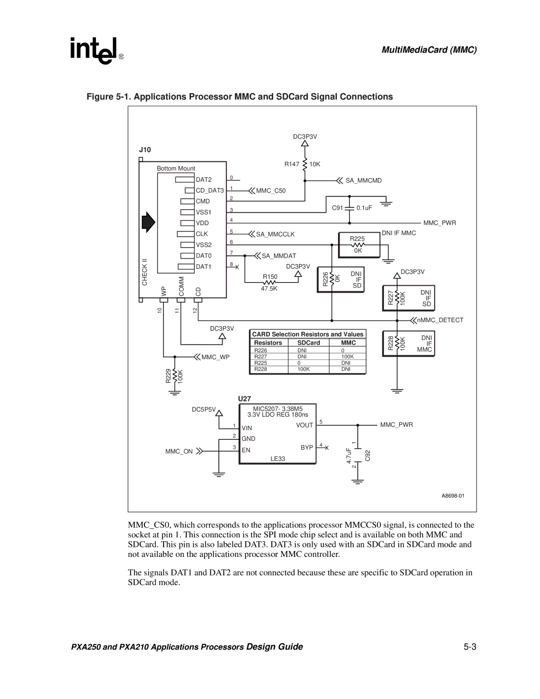
Figure 5-1. Applications Processor MMC and SDCard Signal Connections

J10


Bottom Mount


DAT2


0


CD_DAT3


1


CMD


2


VSS1


3


VDD


4


CLK


5


VSS2


6


II


DAT0


7


8


CHECK


WP


COMM


CD


DAT1


10

11


12


DC3P3V


MMC_WP


R229


100K


DC3P3V


R147

10K


SA_MMCMD

MMC_C50


C91

0.1uF


MMC_PWR

SA_MMCCLK


DNI IF MMC


R225

SA_MMDAT


0K


DC3P3V


DC3P3V

R150

R226

0K

DNI


IF


47.5K


SD


R227

100K

DNI


SD


IF


nMMC_DETECT


CARD Selection Resistors and Values


R228

100K

DNI


R226


DNI


0


MMC


Resistors


SDCard


MMC


IF


R227


DNI


100K


R225


0


DNI


R228


100K


DNI


DC5P5V

MMC_ON

U27

MIC5207- 3.38M5

3.3V LDO REG 180ns

1 VIN

VOUT

2GND

3 EN

BYP


LE33

5

4

4.7uF 2 1

MMC_PWR

C92

A8698-01

MMC_CS0, which corresponds to the applications processor MMCCS0 signal, is connected to the socket at pin 1. This connection is the SPI mode chip select and is available on both MMC and SDCard. This pin is also labeled DAT3. DAT3 is only used with an SDCard in SDCard mode and not available on the applications processor MMC controller.

The signals DAT1 and DAT2 are not connected because these are specific to SDCard operation in SDCard mode.

PXA250 and PXA210 Applications Processors Design Guide

5-3

Page 59
Image 59
Intel PXA250 and PXA210 manual Applications Processor MMC and SDCard Signal Connections

PXA250 and PXA210 specifications

The Intel PXA250 and PXA210 processors, part of the Intel XScale architecture, were introduced in the early 2000s, targeting mobile and embedded applications. They are known for their low power consumption, high performance, and advanced multimedia capabilities, making them suitable for a wide range of devices, including PDAs, smartphones, and other portable computing devices.

The PXA250, which operates at clock speeds ranging from 400 MHz to 624 MHz, features a superscalar architecture that allows it to issue multiple instructions per clock cycle. This enhances the overall performance for demanding applications while maintaining low power usage. It supports a variety of peripheral interfaces, including USB, Ethernet, and various memory types, which contributes to its versatility in different product designs.

One of the key technologies in the PXA250 is the integrated Intel Smart Repeat Technology, which optimizes data processing, thereby reducing the amount of power consumed during operation. This feature is particularly important for battery-powered devices, as it extends the overall battery life, allowing for longer usage times in mobile environments. Additionally, the PXA250 includes a dedicated graphics acceleration unit, which enables enhanced graphics and multimedia performance suited to modern applications at the time.

In contrast, the PXA210 is a more entry-level processor, aimed at cost-sensitive applications. Operating at lower clock speeds, typically around 200 MHz to 400 MHz, it forgoes some of the advanced performance features of the PXA250 while still offering a good balance of performance and power efficiency. The PXA210 is less complex, making it suitable for simpler devices that do not require the extensive capabilities of the PXA250.

Both processors utilize the Intel XScale architecture, which is based on the ARM instruction set. They are built on a 0.13-micron process technology, enabling higher density and lower power consumption compared to their predecessors. With integrated memory controllers and bus interfaces, they facilitate efficient data handling and connectivity options.

In summary, both the Intel PXA250 and PXA210 processors played a crucial role in the evolution of mobile computing by providing powerful processing capabilities with energy efficiency. Their features and technologies enabled device manufacturers to create innovative products that catered to the growing demand for portable devices during that era.