Board Level Overview
Board Level Overview
|
| M88000 |
|
|
|
| 82596CA |
|
|
|
| 53C710 |
|
|
|
| CD2401 |
|
|
|
| PRINTER |
| ||
|
|
|
|
|
| LAN |
|
|
|
|
|
|
|
| SCC |
|
|
|
|
| |||||
|
|
|
|
|
|
|
|
|
| SCSI |
|
|
|
|
|
|
|
| PORT |
| |||||
|
|
|
|
|
|
| ETHERNET |
|
|
|
|
|
|
|
| SERIAL IO |
|
|
|
|
| ||||
|
|
|
|
|
|
|
|
|
|
|
|
|
|
|
|
|
|
|
|
|
|
| |||
|
|
|
|
|
|
|
|
|
|
|
|
|
|
|
|
|
|
|
|
|
|
|
|
|
|
2 |
PCCchip2
|
|
|
|
|
|
|
|
|
|
|
|
|
|
|
|
|
|
|
|
|
|
|
|
|
|
|
|
|
|
|
|
|
|
|
|
| MK48T08 |
| |
|
| DRAM |
|
| VMEchip2 |
|
| EPROM |
|
| BBRAM |
| |||||||
|
|
|
|
|
|
|
|
|
|
|
|
|
|
|
|
| & CLOCK |
| |
|
|
|
|
|
|
|
|
|
|
|
|
|
|
|
|
|
|
|
|
|
|
|
|
|
|
|
|
|
|
|
|
|
|
|
|
|
|
|
|
|
|
|
|
|
|
|
|
|
|
|
|
|
|
|
|
|
|
|
|
VMEbus
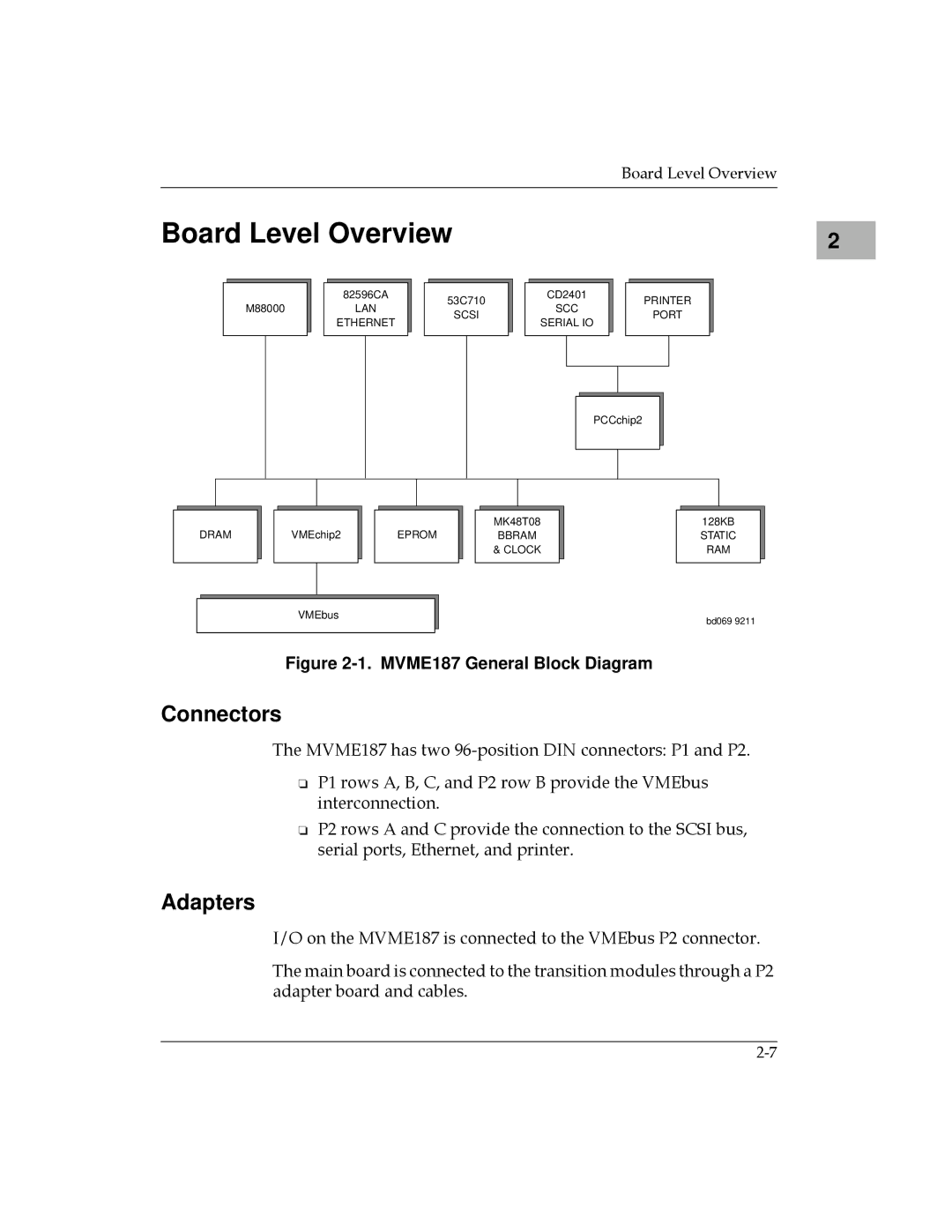
Figure 2-1. MVME187 General Block Diagram
128KB
STATIC
RAM
bd069 9211
Connectors
The MVME187 has two
❏P1 rows A, B, C, and P2 row B provide the VMEbus interconnection.
❏P2 rows A and C provide the connection to the SCSI bus, serial ports, Ethernet, and printer.
Adapters
I/O on the MVME187 is connected to the VMEbus P2 connector.
The main board is connected to the transition modules through a P2 adapter board and cables.