SPRS292A − OCTOBER 2005 − REVISED NOVEMBER 2005
peripheral register descriptions (continued)
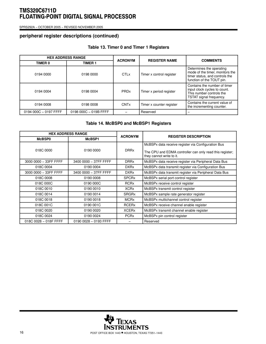
Table 13. Timer 0 and Timer 1 Registers
HEX ADDRESS RANGE | ACRONYM | REGISTER NAME | COMMENTS | ||
|
| ||||
TIMER 0 | TIMER 1 | ||||
|
|
| |||
|
|
|
|
| |
|
|
|
| Determines the operating | |
0194 0000 | 0198 0000 | CTLx | Timer x control register | mode of the timer, monitors the | |
timer status, and controls the | |||||
|
|
|
| ||
|
|
|
| function of the TOUT pin. | |
|
|
|
|
| |
|
|
|
| Contains the number of timer | |
0194 0004 | 0198 0004 | PRDx | Timer x period register | input clock cycles to count. | |
This number controls the | |||||
|
|
|
| ||
|
|
|
| TSTAT signal frequency. | |
|
|
|
|
| |
0194 0008 | 0198 0008 | CNTx | Timer x counter register | Contains the current value of | |
the incrementing counter. | |||||
|
|
|
| ||
|
|
|
|
| |
0194 000C − 0197 FFFF | 0198 000C − 019B FFFF | − | Reserved | − | |
|
|
|
|
| |
Table 14. McBSP0 and McBSP1 Registers
| HEX ADDRESS RANGE | ACRONYM | REGISTER DESCRIPTION | ||
|
|
| |||
McBSP0 | McBSP1 | ||||
|
| ||||
|
|
|
|
| |
|
|
|
| McBSPx data receive register via Configuration Bus | |
018C | 0000 | 0190 0000 | DRRx | The CPU and EDMA controller can only read this register; | |
|
|
|
| ||
|
|
|
| they cannot write to it. | |
|
|
|
| ||
3000 0000 − 33FF FFFF | 3400 0000 − 37FF FFFF | DRRx | McBSPx data receive register via Peripheral Data Bus | ||
|
|
|
|
| |
018C | 0004 | 0190 0004 | DXRx | McBSPx data transmit register via Configuration Bus | |
|
|
|
| ||
3000 0000 − 33FF FFFF | 3400 0000 − 37FF FFFF | DXRx | McBSPx data transmit register via Peripheral Data Bus | ||
|
|
|
|
| |
018C | 0008 | 0190 0008 | SPCRx | McBSPx serial port control register | |
|
|
|
| ||
018C 000C | 0190 000C | RCRx | McBSPx receive control register | ||
|
|
|
|
| |
018C | 0010 | 0190 0010 | XCRx | McBSPx transmit control register | |
|
|
|
|
| |
018C | 0014 | 0190 0014 | SRGRx | McBSPx sample rate generator register | |
|
|
|
|
| |
018C | 0018 | 0190 0018 | MCRx | McBSPx multichannel control register | |
|
|
|
| ||
018C 001C | 0190 001C | RCERx | McBSPx receive channel enable register | ||
|
|
|
|
| |
018C | 0020 | 0190 0020 | XCERx | McBSPx transmit channel enable register | |
|
|
|
|
| |
018C | 0024 | 0190 0024 | PCRx | McBSPx pin control register | |
|
|
|
| ||
018C 0028 − 018F FFFF | 0190 0028 − 0193 FFFF | − | Reserved | ||
16 | POST OFFICE BOX 1443 • HOUSTON, TEXAS 77251−1443 |