SPRS292A − OCTOBER 2005 − REVISED NOVEMBER 2005
cache configuration (CCFG) register description
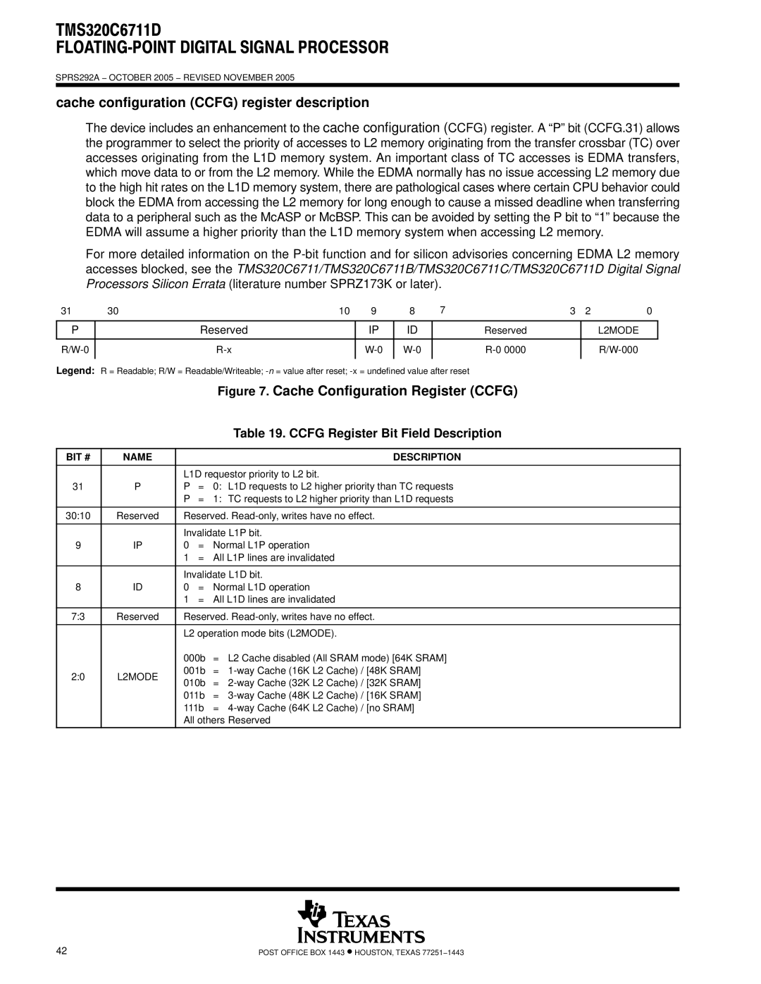
The device includes an enhancement to the cache configuration (CCFG) register. A “P” bit (CCFG.31) allows the programmer to select the priority of accesses to L2 memory originating from the transfer crossbar (TC) over accesses originating from the L1D memory system. An important class of TC accesses is EDMA transfers, which move data to or from the L2 memory. While the EDMA normally has no issue accessing L2 memory due to the high hit rates on the L1D memory system, there are pathological cases where certain CPU behavior could block the EDMA from accessing the L2 memory for long enough to cause a missed deadline when transferring data to a peripheral such as the McASP or McBSP. This can be avoided by setting the P bit to “1” because the EDMA will assume a higher priority than the L1D memory system when accessing L2 memory.
For more detailed information on the
31 | 30 | 10 | 9 | 8 | 7 | 3 | 2 | 0 |
|
|
|
|
|
|
|
|
|
P | Reserved |
| IP | ID | Reserved |
|
| L2MODE |
|
|
|
|
|
|
|
|
|
|
|
| ||||||
|
|
|
|
|
|
|
|
|
Legend: R = Readable; R/W = Readable/Writeable;
Figure 7. Cache Configuration Register (CCFG)
|
|
|
| Table 19. CCFG Register Bit Field Description | ||
|
|
|
|
|
| |
BIT # | NAME |
|
|
| DESCRIPTION | |
|
|
| ||||
|
| L1D requestor priority to L2 bit. | ||||
31 | P | P | = | 0: L1D requests to L2 higher priority than TC requests | ||
|
| P | = | 1: TC requests to L2 higher priority than L1D requests | ||
|
|
| ||||
30:10 | Reserved | Reserved. | ||||
|
|
|
| |||
|
| Invalidate L1P bit. |
| |||
9 | IP | 0 | = | Normal L1P operation |
| |
|
| 1 | = | All L1P lines are invalidated | ||
|
|
|
| |||
|
| Invalidate L1D bit. |
| |||
8 | ID | 0 | = | Normal L1D operation |
| |
|
| 1 | = | All L1D lines are invalidated | ||
|
|
| ||||
7:3 | Reserved | Reserved. | ||||
|
|
| ||||
|
| L2 operation mode bits (L2MODE). | ||||
|
| 000b | = L2 Cache disabled (All SRAM mode) [64K SRAM] | |||
2:0 | L2MODE | 001b | = | L2 Cache) / [48K SRAM] | ||
010b | = | L2 Cache) / [32K SRAM] | ||||
|
| |||||
|
| 011b | = | L2 Cache) / [16K SRAM] | ||
|
| 111b | = | L2 Cache) / [no SRAM] | ||
|
| All others Reserved |
| |||
42 | POST OFFICE BOX 1443 • HOUSTON, TEXAS 77251−1443 |