SPRS292 − OCTOBER 2005
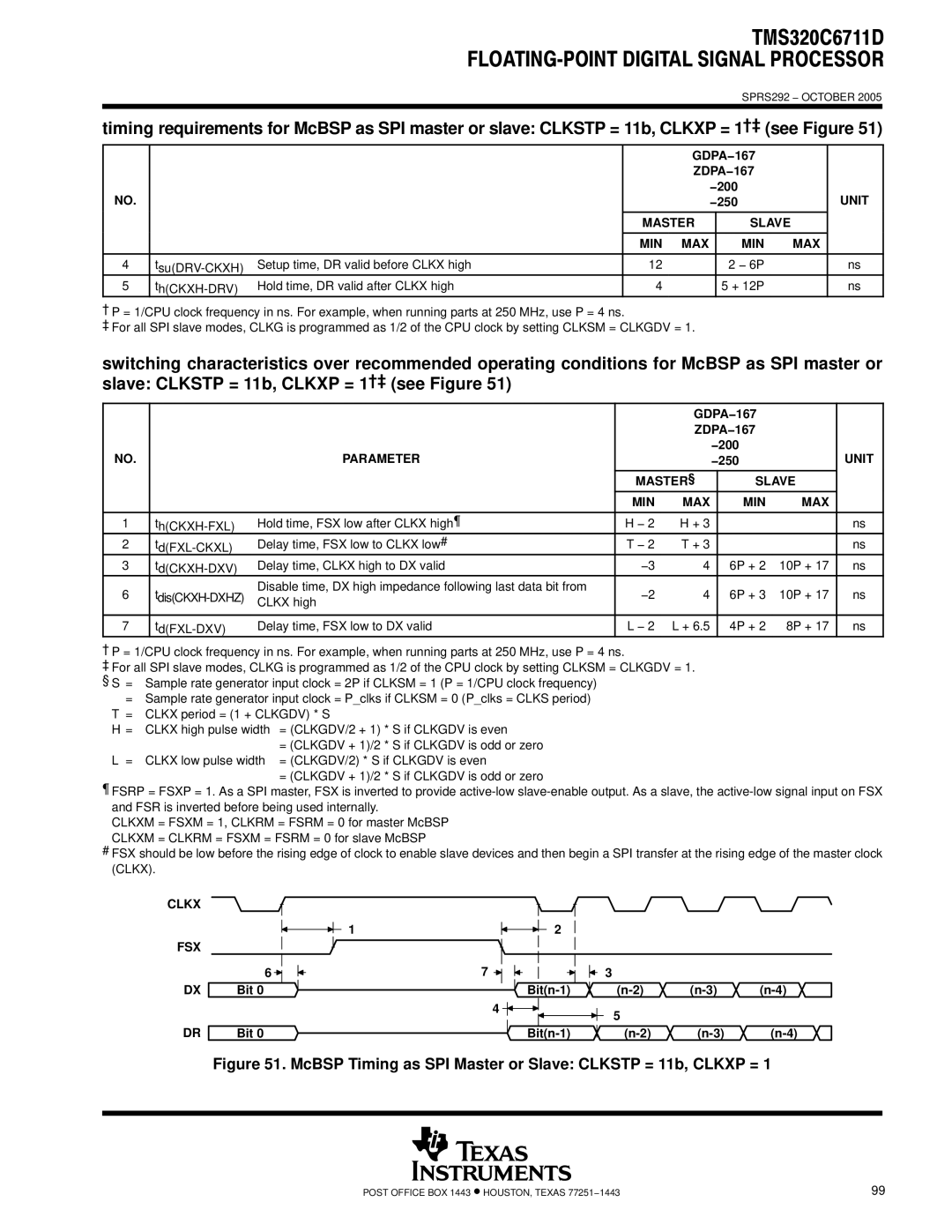
timing requirements for McBSP as SPI master or slave: CLKSTP = 11b, CLKXP = 1†‡ | (see Figure 51) | ||||||
|
|
| GDPA−167 |
|
| ||
|
|
| ZDPA−167 |
|
| ||
NO. |
|
|
| −200 |
| UNIT | |
|
|
| −250 |
| |||
|
|
|
|
|
|
| |
|
|
| MASTER |
| SLAVE |
| |
|
|
|
|
|
|
|
|
|
|
| MIN MAX |
| MIN | MAX |
|
|
|
|
|
|
|
|
|
4 | Setup time, DR valid before CLKX high | 12 |
| 2 − 6P |
| ns | |
5 | Hold time, DR valid after CLKX high | 4 |
| 5 + 12P |
| ns | |
†P = 1/CPU clock frequency in ns. For example, when running parts at 250 MHz, use P = 4 ns.
‡For all SPI slave modes, CLKG is programmed as 1/2 of the CPU clock by setting CLKSM = CLKGDV = 1.
switching characteristics over recommended operating conditions for McBSP as SPI master or slave: CLKSTP = 11b, CLKXP = 1†‡ (see Figure 51)
|
|
|
| GDPA−167 |
|
|
| ||
|
|
|
| ZDPA−167 |
|
|
| ||
NO. |
| PARAMETER |
|
| −200 |
|
| UNIT | |
|
|
| −250 |
|
| ||||
|
|
|
|
|
|
|
| ||
|
|
| MASTER§ |
| SLAVE |
|
| ||
|
|
| MIN | MAX |
| MIN |
| MAX |
|
|
|
|
|
|
|
|
|
|
|
1 | Hold time, FSX low after CLKX high¶ | H − 2 | H + 3 |
|
|
|
| ns | |
2 | Delay time, FSX low to CLKX low# | T − 2 | T + 3 |
|
|
|
| ns | |
3 | Delay time, CLKX high to DX valid | −3 | 4 |
| 6P + 2 | 10P | + 17 | ns | |
6 | Disable time, DX high impedance following last data bit from | −2 | 4 |
| 6P + 3 | 10P | + 17 | ns | |
CLKX high |
| ||||||||
|
|
|
|
|
|
|
|
| |
|
|
|
|
|
|
|
|
|
|
7 | Delay time, FSX low to DX valid | L − 2 | L + 6.5 |
| 4P + 2 | 8P | + 17 | ns | |
†P = 1/CPU clock frequency in ns. For example, when running parts at 250 MHz, use P = 4 ns.
‡For all SPI slave modes, CLKG is programmed as 1/2 of the CPU clock by setting CLKSM = CLKGDV = 1. § S = Sample rate generator input clock = 2P if CLKSM = 1 (P = 1/CPU clock frequency)
=Sample rate generator input clock = P_clks if CLKSM = 0 (P_clks = CLKS period)
T = | CLKX period = (1 + CLKGDV) * S | |
H = | CLKX high pulse width | = (CLKGDV/2 + 1) * S if CLKGDV is even |
|
| = (CLKGDV + 1)/2 * S if CLKGDV is odd or zero |
L = | CLKX low pulse width | = (CLKGDV/2) * S if CLKGDV is even |
=(CLKGDV + 1)/2 * S if CLKGDV is odd or zero
¶FSRP = FSXP = 1. As a SPI master, FSX is inverted to provide
CLKXM = FSXM = 1, CLKRM = FSRM = 0 for master McBSP CLKXM = CLKRM = FSXM = FSRM = 0 for slave McBSP
#FSX should be low before the rising edge of clock to enable slave devices and then begin a SPI transfer at the rising edge of the master clock (CLKX).
CLKX |
|
|
|
|
|
| 1 | 2 |
|
|
|
FSX |
|
|
|
|
|
| 6 | 7 | 3 |
|
|
DX | Bit 0 |
| |||
|
| 4 | 5 |
|
|
|
|
|
|
| |
DR | Bit 0 |
Figure 51. McBSP Timing as SPI Master or Slave: CLKSTP = 11b, CLKXP = 1
POST OFFICE BOX 1443 • HOUSTON, TEXAS 77251−1443 | 99 |