SPRS292A − OCTOBER 2005 − REVISED NOVEMBER 2005
|
|
|
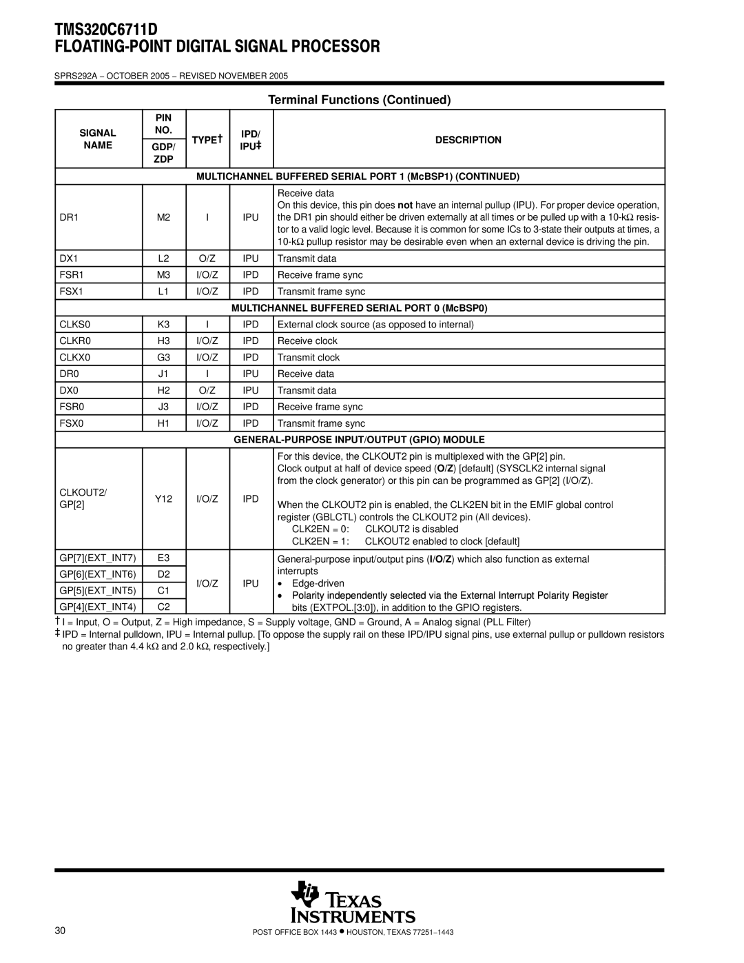
| Terminal Functions (Continued) | |
| PIN |
|
|
|
|
SIGNAL | NO. | TYPE† | IPD/ |
| DESCRIPTION |
|
| ||||
NAME | GDP/ | IPU‡ |
| ||
|
|
| |||
| ZDP |
|
|
|
|
|
|
|
|
| |
|
| MULTICHANNEL BUFFERED SERIAL PORT 1 (McBSP1) (CONTINUED) | |||
|
|
|
|
|
|
|
|
|
|
| Receive data |
|
|
|
|
| On this device, this pin does not have an internal pullup (IPU). For proper device operation, |
DR1 | M2 | I | IPU |
| the DR1 pin should either be driven externally at all times or be pulled up with a |
|
|
|
|
| tor to a valid logic level. Because it is common for some ICs to |
|
|
|
|
| |
|
|
|
|
|
|
DX1 | L2 | O/Z | IPU |
| Transmit data |
|
|
|
|
|
|
FSR1 | M3 | I/O/Z | IPD |
| Receive frame sync |
|
|
|
|
|
|
FSX1 | L1 | I/O/Z | IPD |
| Transmit frame sync |
|
|
|
|
| |
|
|
| MULTICHANNEL BUFFERED SERIAL PORT 0 (McBSP0) | ||
|
|
|
|
|
|
CLKS0 | K3 | I | IPD |
| External clock source (as opposed to internal) |
|
|
|
|
|
|
CLKR0 | H3 | I/O/Z | IPD |
| Receive clock |
|
|
|
|
|
|
CLKX0 | G3 | I/O/Z | IPD |
| Transmit clock |
|
|
|
|
|
|
DR0 | J1 | I | IPU |
| Receive data |
|
|
|
|
|
|
DX0 | H2 | O/Z | IPU |
| Transmit data |
|
|
|
|
|
|
FSR0 | J3 | I/O/Z | IPD |
| Receive frame sync |
|
|
|
|
|
|
FSX0 | H1 | I/O/Z | IPD |
| Transmit frame sync |
|
|
|
|
| |
|
|
|
| ||
|
|
|
|
|
|
|
|
|
|
| For this device, the CLKOUT2 pin is multiplexed with the GP[2] pin. |
|
|
|
|
| Clock output at half of device speed (O/Z) [default] (SYSCLK2 internal signal |
|
|
|
|
| from the clock generator) or this pin can be programmed as GP[2] (I/O/Z). |
CLKOUT2/ | Y12 | I/O/Z | IPD |
|
|
GP[2] |
| When the CLKOUT2 pin is enabled, the CLK2EN bit in the EMIF global control | |||
|
|
|
| ||
|
|
|
|
| register (GBLCTL) controls the CLKOUT2 pin (All devices). |
|
|
|
|
| CLK2EN = 0: CLKOUT2 is disabled |
|
|
|
|
| CLK2EN = 1: CLKOUT2 enabled to clock [default] |
|
|
|
|
|
|
GP[7](EXT_INT7) | E3 |
|
|
| |
GP[6](EXT_INT6) | D2 |
|
|
| interrupts |
I/O/Z | IPU |
| • | ||
|
|
| |||
GP[5](EXT_INT5) | C1 |
| |||
|
|
| • Polarity independently selected via the External Interrupt Polarity Register | ||
|
|
|
|
| |
GP[4](EXT_INT4) | C2 |
|
|
| bits (EXTPOL.[3:0]), in addition to the GPIO registers. |
†I = Input, O = Output, Z = High impedance, S = Supply voltage, GND = Ground, A = Analog signal (PLL Filter)
‡IPD = Internal pulldown, IPU = Internal pullup. [To oppose the supply rail on these IPD/IPU signal pins, use external pullup or pulldown resistors no greater than 4.4 kΩ and 2.0 kΩ, respectively.]
30 | POST OFFICE BOX 1443 • HOUSTON, TEXAS 77251−1443 |