SPRS292A − OCTOBER 2005 − REVISED NOVEMBER 2005 |
|
|
|
|
|
| |||
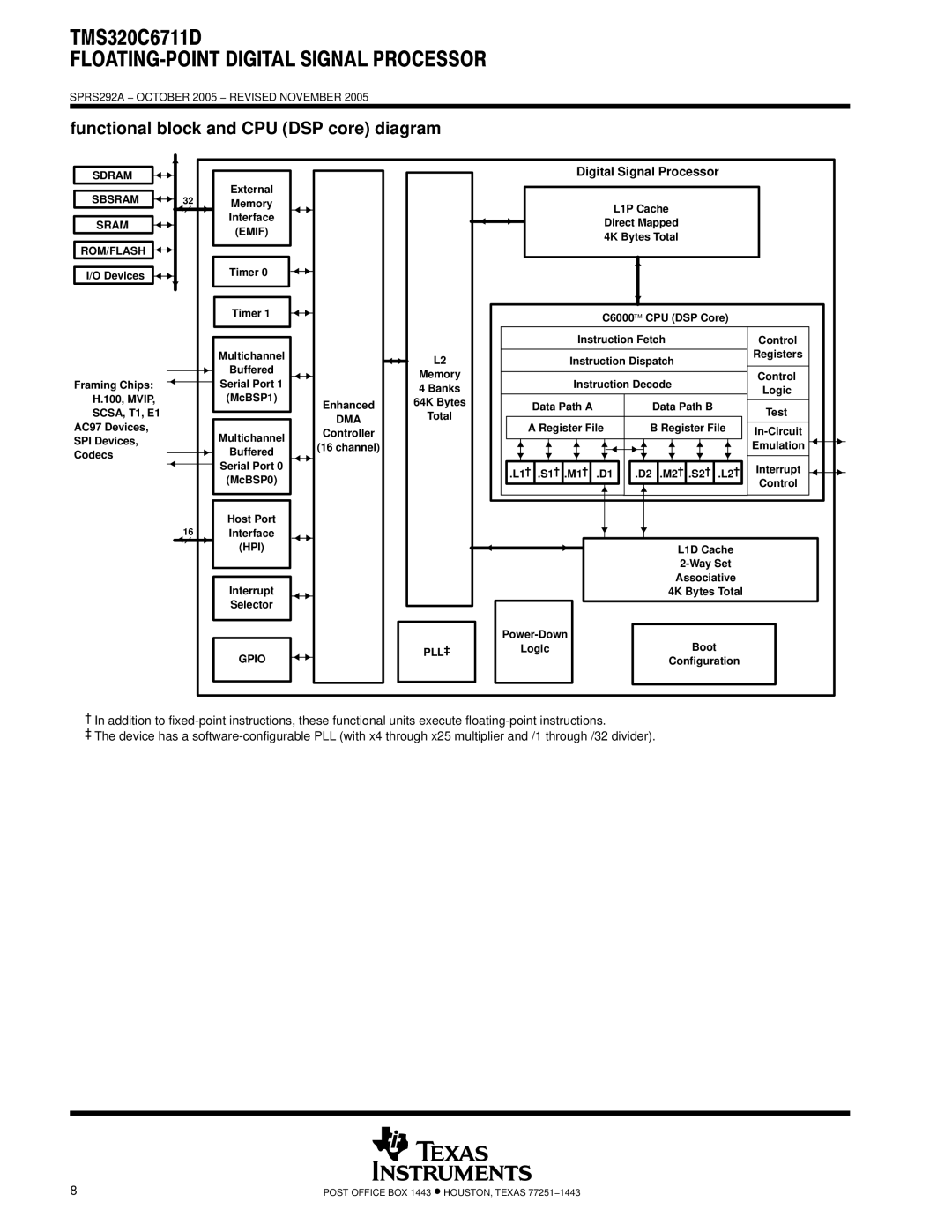
functional block and CPU (DSP core) diagram |
|
|
|
|
| ||||
SDRAM |
|
|
|
|
|
| Digital Signal Processor |
| |
SBSRAM | 32 | External |
|
|
|
|
|
|
|
Memory |
|
|
|
|
| L1P Cache |
| ||
|
|
|
|
|
|
|
| ||
|
| Interface |
|
|
|
|
|
| |
SRAM |
|
|
|
|
| Direct Mapped |
| ||
| (EMIF) |
|
|
|
|
| |||
|
|
|
|
|
| 4K Bytes Total |
| ||
|
|
|
|
|
|
|
| ||
ROM/FLASH |
|
|
|
|
|
|
|
|
|
I/O Devices |
| Timer 0 |
|
|
|
|
|
|
|
|
|
|
|
|
|
|
|
| |
|
| Timer 1 |
|
|
|
| C6000 CPU (DSP Core) |
| |
|
|
|
|
|
|
|
| ||
|
|
|
|
|
|
| Instruction Fetch | Control | |
|
| Multichannel |
| L2 |
|
| Instruction Dispatch | Registers | |
|
| Buffered |
|
|
|
| |||
|
|
| Memory |
|
|
|
| Control | |
Framing Chips: |
| Serial Port 1 |
|
|
| Instruction Decode | |||
|
| 4 Banks |
|
| Logic | ||||
H.100, MVIP, |
| (McBSP1) |
|
|
|
|
| ||
| Enhanced | 64K Bytes |
| Data Path A | Data Path B |
| |||
SCSA, T1, E1 |
|
|
| Test | |||||
|
| DMA | Total |
|
|
|
| ||
AC97 Devices, |
|
| A Register File | B Register File | |||||
| Multichannel | Controller |
| ||||||
SPI Devices, |
|
|
|
|
|
| |||
| (16 channel) |
|
|
|
|
| Emulation | ||
Codecs |
| Buffered |
|
|
|
|
| ||
|
|
|
|
|
|
|
| ||
|
| Serial Port 0 |
|
| .L1† | .S1† | .M1† .D1 | .D2 .M2† .S2† .L2† | Interrupt |
|
| (McBSP0) |
|
| |||||
|
|
|
|
|
|
|
| Control | |
|
|
|
|
|
|
|
|
| |
|
| Host Port |
|
|
|
|
|
|
|
| 16 | Interface |
|
|
|
|
|
|
|
|
| (HPI) |
|
|
|
|
| L1D Cache |
|
|
|
|
|
|
|
|
|
| |
|
|
|
|
|
|
|
| Associative |
|
|
| Interrupt |
|
|
|
|
| 4K Bytes Total |
|
|
| Selector |
|
|
|
|
|
|
|
|
|
|
|
| Boot |
| |||
|
| GPIO |
| PLL‡ | Logic |
|
| ||
|
|
|
|
|
|
| Configuration |
| |
†In addition to
‡The device has a
8 | POST OFFICE BOX 1443 • HOUSTON, TEXAS 77251−1443 |