SPRS292A − OCTOBER 2005 − REVISED NOVEMBER 2005
PLL and PLL controller (continued)
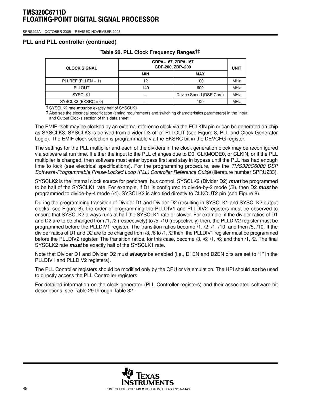
Table 28. PLL Clock Frequency Ranges†‡
|
| GDPA−167, |
| |
CLOCK SIGNAL |
| UNIT | ||
|
|
| ||
| MIN |
| MAX |
|
|
|
|
|
|
PLLREF (PLLEN = 1) | 12 |
| 100 | MHz |
|
|
|
|
|
PLLOUT | 140 |
| 600 | MHz |
|
|
|
|
|
SYSCLK1 | − |
| Device Speed (DSP Core) | MHz |
|
|
|
|
|
SYSCLK3 (EKSRC = 0) | − |
| 100 | MHz |
†SYSCLK2 rate must be exactly half of SYSCLK1.
‡Also see the electrical specification (timing requirements and switching characteristics parameters) in the Input and Output Clocks section of this data sheet.
The EMIF itself may be clocked by an external reference clock via the ECLKIN pin or can be generated
The settings for the PLL multiplier and each of the dividers in the clock generation block may be reconfigured via software at run time. If either the input to the PLL changes due to D0, CLKMODE0, or CLKIN, or if the PLL multiplier is changed, then software must enter bypass first and stay in bypass until the PLL has had enough time to lock (see electrical specifications). For the programming procedure, see the TMS320C6000 DSP
SYSCLK2 is the internal clock source for peripheral bus control. SYSCLK2 (Divider D2) must be programmed to be half of the SYSCLK1 rate. For example, if D1 is configured to
During the programming transition of Divider D1 and Divider D2 (resulting in SYSCLK1 and SYSCLK2 output clocks, see Figure 8), the order of programming the PLLDIV1 and PLLDIV2 registers must be observed to ensure that SYSCLK2 always runs at half the SYSCLK1 rate or slower. For example, if the divider ratios of D1 and D2 are to be changed from /1, /2 (respectively) to /5, /10 (respectively) then, the PLLDIV2 register must be programmed before the PLLDIV1 register. The transition ratios become /1, /2; /1, /10; and then /5, /10. If the divider ratios of D1 and D2 are to be changed from /3, /6 to /1, /2 then, the PLLDIV1 register must be programmed before the PLLDIV2 register. The transition ratios, for this case, become /3, /6; /1, /6; and then /1, /2. The final SYSCLK2 rate must be exactly half of the SYSCLK1 rate.
Note that Divider D1 and Divider D2 must always be enabled (i.e., D1EN and D2EN bits are set to “1” in the PLLDIV1 and PLLDIV2 registers).
The PLL Controller registers should be modified only by the CPU or via emulation. The HPI should not be used to directly access the PLL Controller registers.
For detailed information on the clock generator (PLL Controller registers) and their associated software bit descriptions, see Table 29 through Table 32.
48 | POST OFFICE BOX 1443 • HOUSTON, TEXAS 77251−1443 |