SPRS292A − OCTOBER 2005 − REVISED NOVEMBER 2005
PLL and PLL controller
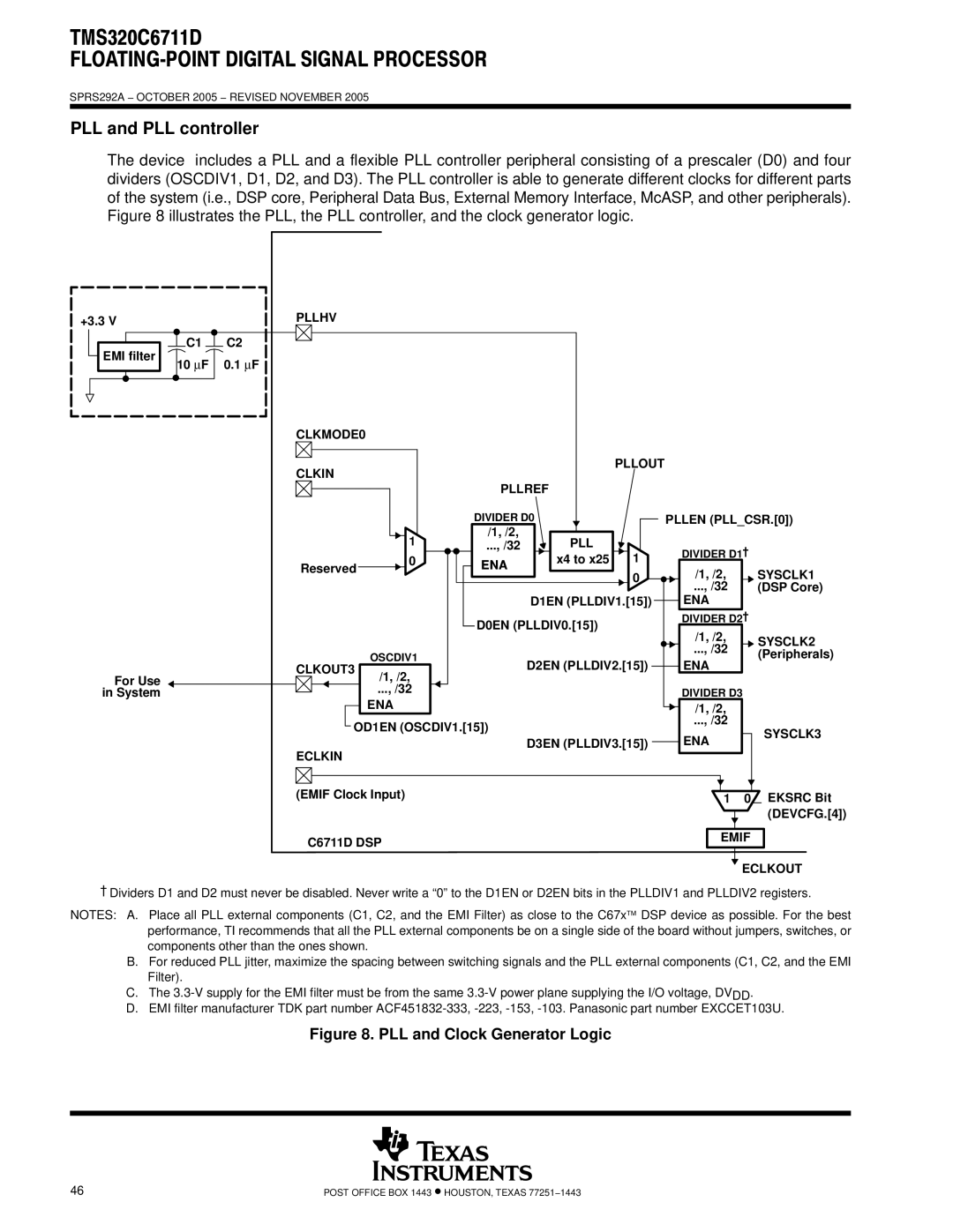
The device includes a PLL and a flexible PLL controller peripheral consisting of a prescaler (D0) and four dividers (OSCDIV1, D1, D2, and D3). The PLL controller is able to generate different clocks for different parts of the system (i.e., DSP core, Peripheral Data Bus, External Memory Interface, McASP, and other peripherals). Figure 8 illustrates the PLL, the PLL controller, and the clock generator logic.
+3.3 V
![]() EMI filter
EMI filter
For Use in System
C1 C2
10 ∝F 0.1 ∝F
PLLHV
CLKMODE0 |
|
|
|
|
|
|
|
CLKIN |
|
|
| PLLOUT |
|
|
|
|
|
|
|
|
|
| |
|
| PLLREF |
|
|
|
| |
|
| DIVIDER D0 |
| PLLEN (PLL_CSR.[0]) | |||
| 1 | /1, /2, | PLL |
|
|
|
|
| ..., /32 | 1 | DIVIDER D1† |
| |||
| 0 | ENA | x4 to x25 |
| |||
Reserved | /1, /2, |
| SYSCLK1 | ||||
|
| 0 |
| ||||
|
|
|
|
| |||
|
|
|
|
| ..., /32 |
| (DSP Core) |
|
|
| D1EN (PLLDIV1.[15]) | ENA |
|
| |
|
| D0EN (PLLDIV0.[15]) |
| DIVIDER D2† |
| ||
|
|
| /1, /2, |
|
| ||
|
|
|
|
|
| SYSCLK2 | |
|
|
|
|
| ..., /32 |
| |
| OSCDIV1 |
|
|
|
| (Peripherals) | |
CLKOUT3 |
| D2EN (PLLDIV2.[15]) | ENA |
| |||
/1, /2, |
|
|
| ||||
|
|
|
|
|
|
| |
| ..., /32 |
|
|
| DIVIDER D3 |
| |
| ENA |
|
|
|
| ||
|
|
|
| /1, /2, |
|
| |
OD1EN (OSCDIV1.[15]) |
|
| ..., /32 |
| SYSCLK3 | ||
|
| ENA |
| ||||
|
|
| D3EN (PLLDIV3.[15]) |
| |||
ECLKIN |
|
|
|
| |||
|
|
|
|
|
|
| |
(EMIF Clock Input) |
|
|
| 1 | 0 | EKSRC Bit | |
|
|
|
|
|
|
| (DEVCFG.[4]) |
C6711D DSP |
|
|
| EMIF |
| ||
|
|
|
|
|
| ||
|
|
|
|
|
| ECLKOUT | |
†Dividers D1 and D2 must never be disabled. Never write a “0” to the D1EN or D2EN bits in the PLLDIV1 and PLLDIV2 registers.
NOTES: A. Place all PLL external components (C1, C2, and the EMI Filter) as close to the C67x DSP device as possible. For the best performance, TI recommends that all the PLL external components be on a single side of the board without jumpers, switches, or components other than the ones shown.
B.For reduced PLL jitter, maximize the spacing between switching signals and the PLL external components (C1, C2, and the EMI Filter).
C.The
D.EMI filter manufacturer TDK part number
Figure 8. PLL and Clock Generator Logic
46 | POST OFFICE BOX 1443 • HOUSTON, TEXAS 77251−1443 |