SPRS292A − OCTOBER 2005 − REVISED NOVEMBER 2005
PLL and PLL controller (continued)
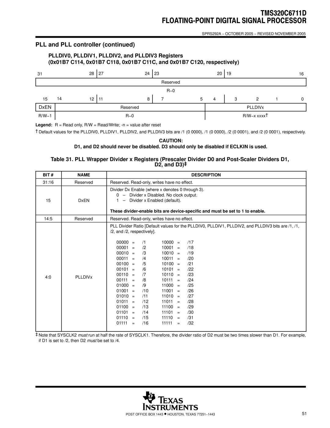
PLLDIV0, PLLDIV1, PLLDIV2, and PLLDIV3 Registers
(0x01B7 C114, 0x01B7 C118, 0x01B7 C11C, and 0x01B7 C120, respectively)
31 |
| 28 | 27 | 24 | 23 |
| 20 | 19 |
|
| 16 |
|
|
|
|
|
|
|
|
|
|
|
|
|
|
|
|
| Reserved |
|
|
|
|
|
|
|
|
|
|
|
|
|
|
|
|
|
|
|
|
|
|
| R−0 |
|
|
|
|
|
|
15 | 14 | 12 |
| 8 |
| 5 | 4 |
| 2 | 1 | 0 |
11 | 7 | 3 | |||||||||
|
|
|
|
|
|
|
|
|
|
|
|
DxEN |
|
|
| Reserved |
|
|
|
| PLLDIVx |
|
|
|
|
|
|
|
|
|
|
|
|
|
|
R/W−1 |
|
|
| R−0 |
|
|
|
| R/W−x xxxx † |
|
|
Legend: R = Read only, R/W = Read/Write;
†Default values for the PLLDIV0, PLLDIV1, PLLDIV2, and PLLDIV3 bits are /1 (0 0000), /1 (0 0000), /2 (0 0001), and /2 (0 0001), respectively.
CAUTION:
D1, and D2 should never be disabled. D3 should only be disabled if ECLKIN is used.
Table 31. PLL Wrapper Divider x Registers (Prescaler Divider D0 and
D2, and D3)‡
BIT # | NAME |
|
| DESCRIPTION |
31:16 | Reserved | Reserved. | ||
|
|
| ||
|
| Divider Dx Enable (where x denotes 0 through 3). | ||
|
| 0 | – | Divider x Disabled. No clock output. |
15 | DxEN | 1 | – | Divider x Enabled (default). |
|
| These | ||||||
14:5 | Reserved | Reserved. | ||||||
|
|
| ||||||
|
| PLL Divider Ratio [Default values for the PLLDIV0, PLLDIV1, PLLDIV2, and PLLDIV3 bits are /1, /1, | ||||||
|
| /2, and /2, respectively]. |
|
|
| |||
|
| 00000 | = | /1 | 10000 | = | /17 | |
|
| 00001 | = | /2 | 10001 | = | /18 | |
|
| 00010 | = | /3 | 10010 | = | /19 | |
|
| 00011 | = | /4 | 10011 | = | /20 | |
|
| 00100 | = | /5 | 10100 | = | /21 | |
|
| 00101 | = | /6 | 10101 | = | /22 | |
4:0 | PLLDIVx | 00110 | = | /7 | 10110 | = | /23 | |
00111 | = | /8 | 10111 | = | /24 | |||
|
| |||||||
|
| 01000 | = | /9 | 11000 | = | /25 | |
|
| 01001 | = | /10 | 11001 | = | /26 | |
|
| 01010 | = | /11 | 11010 | = | /27 | |
|
| 01011 | = | /12 | 11011 | = | /28 | |
|
| 01100 | = | /13 | 11100 | = | /29 | |
|
| 01101 | = | /14 | 11101 | = | /30 | |
|
| 01110 | = | /15 | 11110 | = | /31 | |
|
| 01111 | = | /16 | 11111 | = | /32 | |
‡Note that SYSCLK2 must run at half the rate of SYSCLK1. Therefore, the divider ratio of D2 must be two times slower than D1. For example, if D1 is set to /2, then D2 must be set to /4.
POST OFFICE BOX 1443 • HOUSTON, TEXAS 77251−1443 | 51 |