SPRS292A − OCTOBER 2005 − REVISED NOVEMBER 2005
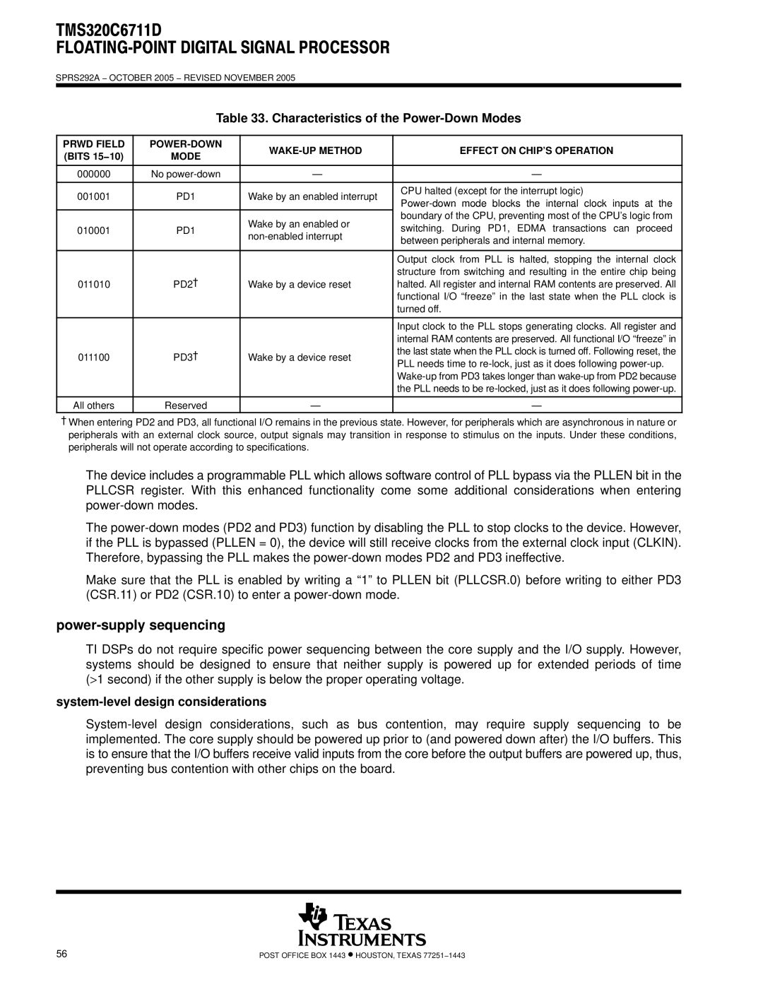
Table 33. Characteristics of the Power-Down Modes
PRWD FIELD | EFFECT ON CHIP’S OPERATION | |||
(BITS 15−10) | MODE | |||
|
| |||
|
|
|
| |
000000 | No | — | — | |
|
|
|
| |
001001 | PD1 | Wake by an enabled interrupt | CPU halted (except for the interrupt logic) | |
|
|
| ||
|
| Wake by an enabled or | boundary of the CPU, preventing most of the CPU’s logic from | |
010001 | PD1 | switching. During PD1, EDMA transactions can proceed | ||
|
| between peripherals and internal memory. | ||
|
|
| ||
|
|
|
| |
|
|
| Output clock from PLL is halted, stopping the internal clock | |
| PD2† |
| structure from switching and resulting in the entire chip being | |
011010 | Wake by a device reset | halted. All register and internal RAM contents are preserved. All | ||
|
|
| functional I/O “freeze” in the last state when the PLL clock is | |
|
|
| turned off. | |
|
|
|
| |
|
|
| Input clock to the PLL stops generating clocks. All register and | |
|
|
| internal RAM contents are preserved. All functional I/O “freeze” in | |
011100 | PD3† | Wake by a device reset | the last state when the PLL clock is turned off. Following reset, the | |
PLL needs time to | ||||
|
|
| ||
|
|
| ||
|
|
| the PLL needs to be | |
|
|
|
| |
All others | Reserved | — | — |
†When entering PD2 and PD3, all functional I/O remains in the previous state. However, for peripherals which are asynchronous in nature or peripherals with an external clock source, output signals may transition in response to stimulus on the inputs. Under these conditions, peripherals will not operate according to specifications.
The device includes a programmable PLL which allows software control of PLL bypass via the PLLEN bit in the PLLCSR register. With this enhanced functionality come some additional considerations when entering
The
Make sure that the PLL is enabled by writing a “1” to PLLEN bit (PLLCSR.0) before writing to either PD3 (CSR.11) or PD2 (CSR.10) to enter a
power-supply sequencing
TI DSPs do not require specific power sequencing between the core supply and the I/O supply. However, systems should be designed to ensure that neither supply is powered up for extended periods of time (>1 second) if the other supply is below the proper operating voltage.
system-level design considerations
56 | POST OFFICE BOX 1443 • HOUSTON, TEXAS 77251−1443 |