Motorola TMS320C6711D warranty Pwrd Field of the CSR Register, PD3 PD2 PD1

Models: TMS320C6711D

1 107
Download 107 pages 8.75 Kb
Page 55
Image 55

SPRS292A − OCTOBER 2005 − REVISED NOVEMBER 2005

31

16


15

14

13

12

11

10

9

8


Enable or

Enabled


Reserved

Non-Enabled

PD3

PD2

PD1


Interrupt Wake


Interrupt Wake


R/W-0

R/W-0

R/W-0

R/W-0

R/W-0

R/W-0


7


0


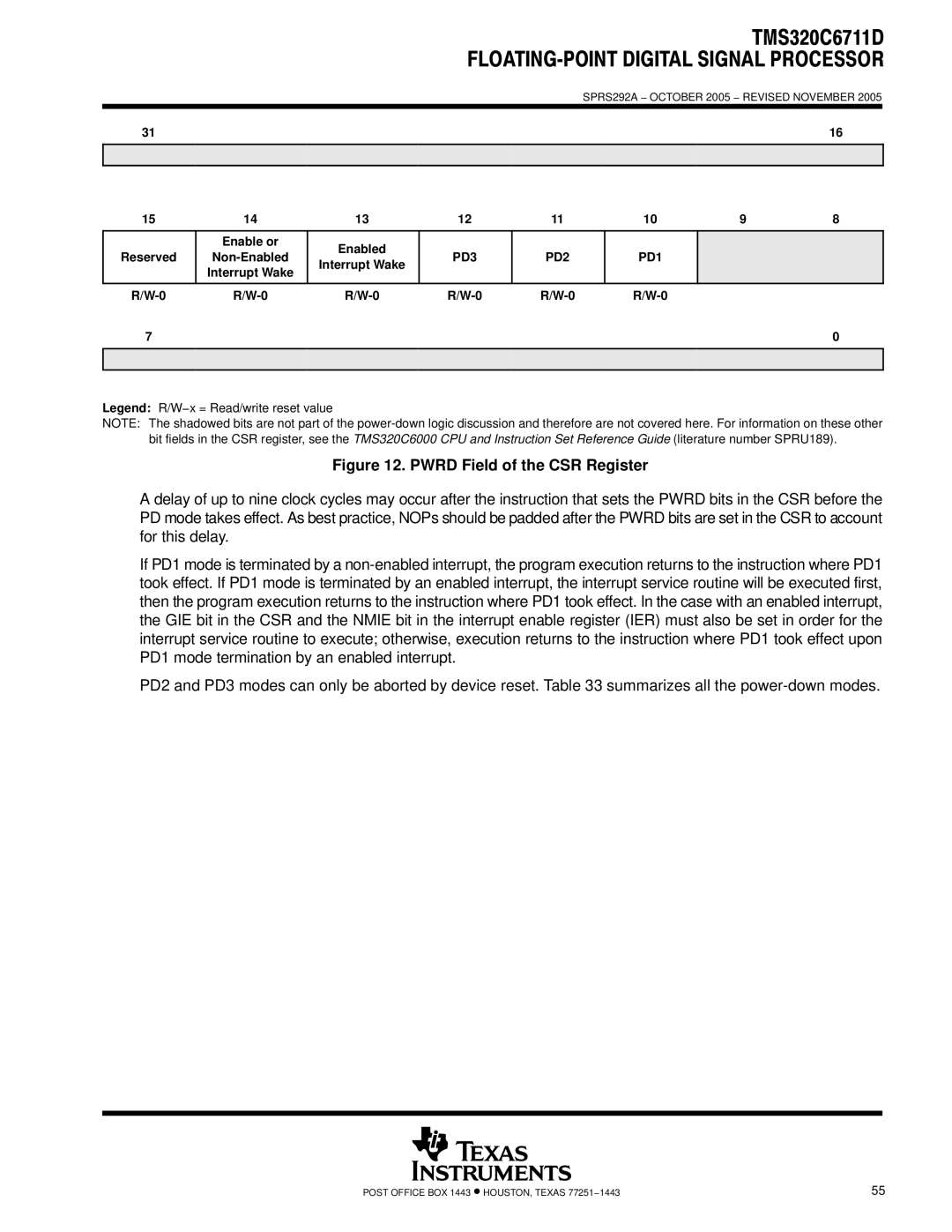
Legend: R/W−x = Read/write reset value

NOTE: The shadowed bits are not part of the power-down logic discussion and therefore are not covered here. For information on these other

bit fields in the CSR register, see the TMS320C6000 CPU and Instruction Set Reference Guide (literature number SPRU189).

Figure 12. PWRD Field of the CSR Register

A delay of up to nine clock cycles may occur after the instruction that sets the PWRD bits in the CSR before the PD mode takes effect. As best practice, NOPs should be padded after the PWRD bits are set in the CSR to account for this delay.

If PD1 mode is terminated by a non-enabled interrupt, the program execution returns to the instruction where PD1 took effect. If PD1 mode is terminated by an enabled interrupt, the interrupt service routine will be executed first, then the program execution returns to the instruction where PD1 took effect. In the case with an enabled interrupt, the GIE bit in the CSR and the NMIE bit in the interrupt enable register (IER) must also be set in order for the interrupt service routine to execute; otherwise, execution returns to the instruction where PD1 took effect upon PD1 mode termination by an enabled interrupt.

PD2 and PD3 modes can only be aborted by device reset. Table 33 summarizes all the power-down modes.

POST OFFICE BOX 1443 HOUSTON, TEXAS 77251−1443

55

Page 55
Image 55
Motorola TMS320C6711D warranty Pwrd Field of the CSR Register, PD3 PD2 PD1